· AtlasPCB Engineering · Engineering · 9 min read
PCB DFM Check for HDI Designs: Microvia Stacking Rules and Fabrication Constraints Your EDA Tool Misses
A practical DFM checklist for HDI PCB designs covering microvia stacking limits, aspect ratio constraints, annular ring requirements, and sequential lamination rules that most EDA design rule checks do not flag.
Quick Answer
EDA tools check trace/space and annular ring but miss critical HDI fabrication constraints — maximum microvia stack height (2 for standard, 3 with fill-and-cap), aspect ratio limits for laser-drilled vias (0.8:1 for 0.1mm vias), and sequential lamination registration tolerances that affect pad capture — resulting in 35% of first-time HDI orders requiring redesign before fabrication.
Quick Answer: The HDI DFM Gaps Your EDA Tool Does Not Cover
| DFM Constraint | EDA Tool Checks? | Fabricator Requires |
|---|---|---|
| Microvia stack height limit | No | Max 2 (standard) or 3 (filled+capped) |
| Microvia aspect ratio (depth:diameter) | No | 0.8:1 maximum for 0.1mm vias |
| Sequential lamination registration | No | +/-50um per cycle added to pad size |
| Via-in-pad fill planarity | No | Less than 10um concavity for SMD pads |
| Minimum annular ring after registration | Partially | 75um minimum after all tolerances |
| Copper balance between lamination pairs | No | Less than 20% differential per layer pair |
In our production data from the first half of 2026, 35% of first-time HDI orders arrive with at least one DFM constraint violation that EDA design rule checking did not flag. The most expensive violations — those requiring actual layout changes rather than simple process adjustments — involve microvia stacking configurations that cannot be reliably manufactured and pad sizes that lose capture after sequential lamination registration shifts accumulate.
Why EDA Design Rule Checks Are Insufficient for HDI
Standard EDA design rule checking was developed for conventional through-hole PCB technology. It validates what can be measured from Gerber files: trace width and spacing, annular ring around drills, minimum drill sizes, and copper-to-edge clearances. These checks work well for standard multilayer boards where a single lamination cycle produces the finished product.
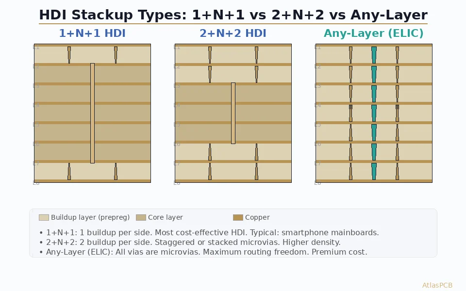
HDI fabrication fundamentally changes the manufacturing paradigm. A 2+N+2 buildup requires three separate lamination cycles — the core lamination, then one sequential lamination on each side. Each cycle introduces independent registration error between the new layer and the existing structure. An EDA tool that checks annular ring against the nominal pad position has no mechanism to account for the cumulative registration shift that occurs when layer 1 was drilled relative to a core whose position shifted 30um in X during the second lamination press cycle.
Our process engineering team tracks registration capability at Cpk > 1.33 for each sequential lamination step, with typical sigma of 25um in both X and Y. For a 2+N+2 buildup, the total registration uncertainty between the outermost microvia and the inner core target pad is approximately 50um — meaning a designer who specifies a 0.25mm pad for a 0.1mm microvia with “plenty” of 75um annular ring actually has only 25um of margin after worst-case registration. That is below our minimum acceptable annular ring of 50um, and the design will either be rejected or run with elevated risk of microvia breakout.
The practical implication: every HDI design should add the manufacturer’s stated registration tolerance to the minimum annular ring requirement for each sequential lamination boundary that the via crosses. A via spanning two sequential laminations needs twice the registration budget of one that stays within a single buildup layer.
HDI PCB MANUFACTURER
Free DFM Review for HDI Designs
Upload your Gerber files. Our HDI process engineers check microvia stacking, registration budgets, and aspect ratios before you commit to fabrication.
Upload for DFM Review ›
Microvia Stacking: The Rules Your Fabricator Enforces
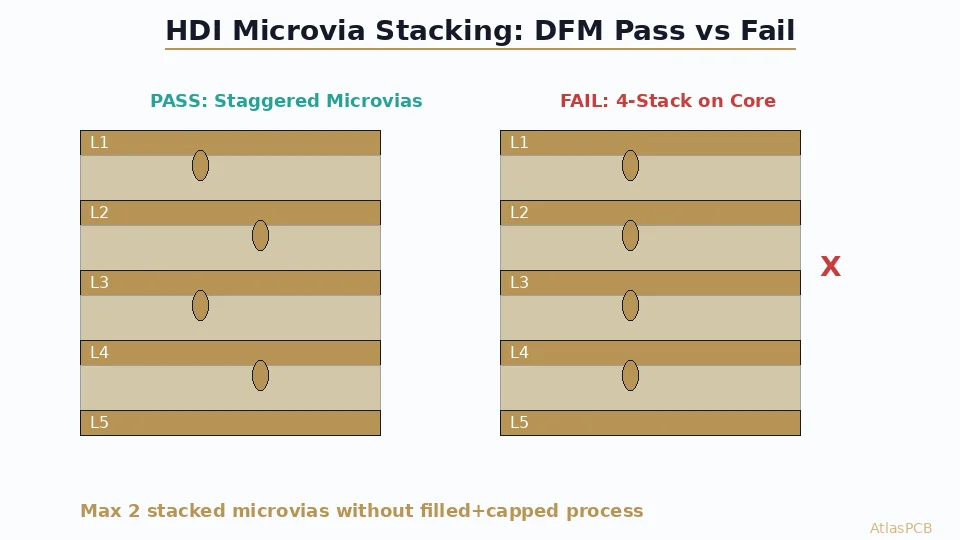
The maximum number of microvias you can reliably stack directly on top of each other depends on whether the underlying via is filled and planarized before the next lamination cycle. Without fill-and-cap processing, each subsequent microvia is laser-drilled into a depression — the unfilled void of the previous microvia. This creates progressively worse copper plating coverage in the via barrel, eventually resulting in a void or weak copper connection that passes electrical test but fails under thermal cycling.
For standard HDI processes without via fill, the maximum reliable stack is 2 microvias. The first microvia drills into solid copper on a core layer. The second microvia drills into the plated copper cap of the first — which is essentially a flat target. A third microvia attempting to drill into the plated cap of a second unfilled microvia finds an uneven surface with potential dimples from incomplete fill, and the laser ablation quality degrades significantly.
With filled-and-capped processing (conductive or non-conductive epoxy fill followed by surface planarization to less than 10um), each microvia becomes a solid target for the next. This enables stacking to 3-4 levels in high-end processes, though each fill-and-cap cycle adds approximately $5-12 per board in processing cost and requires an additional 2-3 days of production time.
The critical DFM check that EDA tools miss: if your design specifies a via stack transitioning from L1 through L2, L3, and landing on L4 in a 3+N+3 buildup, does each intermediate via get filled before the next lamination? If not, the fabricator will either reject the design or reduce it to a staggered configuration — which requires different pad locations on each layer and may not fit your routing density requirements.
Aspect Ratio Constraints for Laser-Drilled Vias
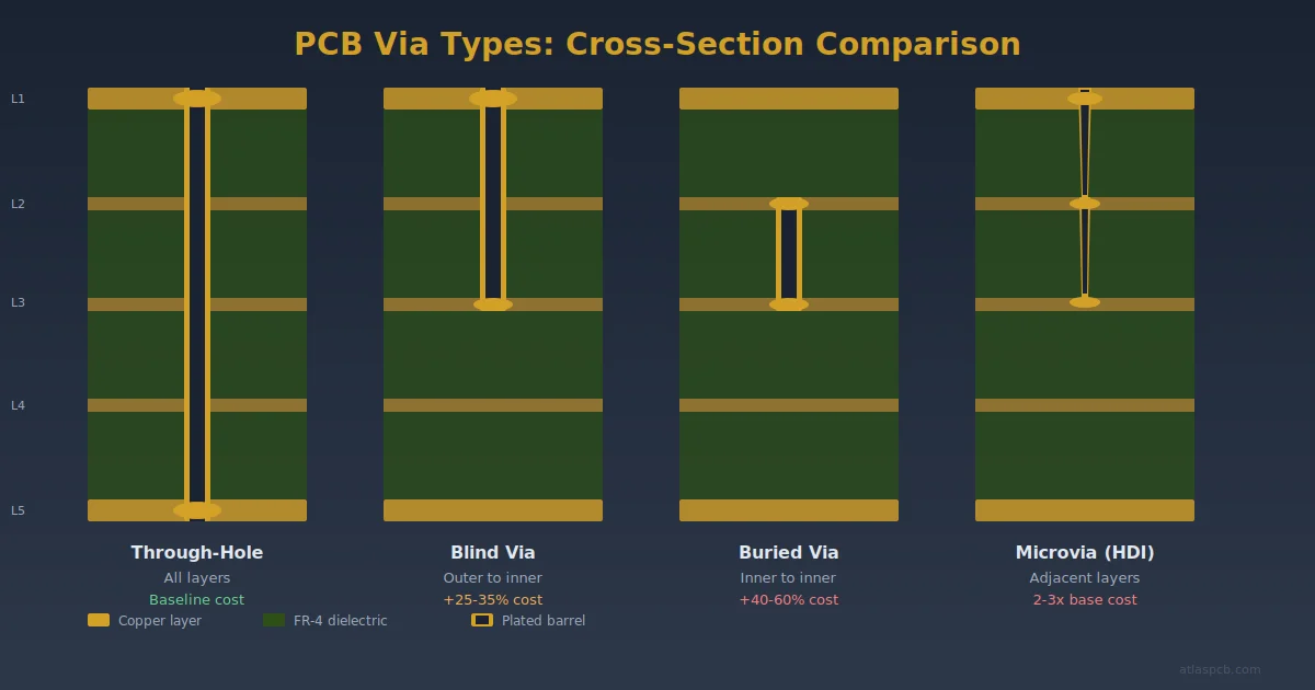
Laser drilling for microvias operates under physical constraints that differ fundamentally from mechanical drilling. A CO2 laser ablates dielectric material and stops on the copper target pad below. The achievable depth-to-diameter ratio is limited by the laser beam divergence, the plasma evacuation from the hole during drilling, and the ability to completely remove dielectric residue (desmear) from the bottom of a high-aspect-ratio hole.
The practical limit for standard CO2 laser drilling is 0.8:1 aspect ratio. For the most common microvia diameter of 0.1mm (100um), this means a maximum depth of approximately 80um — which corresponds to one layer of prepreg (typically 60-75um after pressing). If your stackup uses a thick prepreg or bondply between sequential layers (say, 100um), a 0.1mm microvia cannot reliably reach the target pad below. The solution is either increasing the via diameter to 0.125mm or 0.15mm, or specifying a thinner prepreg layer in the buildup.
UV laser systems achieve slightly better aspect ratios (up to 1:1) at smaller diameters, but the processing speed drops significantly and cost increases. For designs requiring 75um or 50um microvias — typical for any-layer HDI with 0.4mm-pitch BGA breakout — the dielectric thickness between sequential layers must be held below 75um or 50um respectively.
We run incoming thickness measurement on all prepreg materials and adjust lamination parameters to achieve target pressed thickness within +/-5um. This level of control is necessary because the designer’s impedance model and the microvia aspect ratio calculation both depend on knowing the actual dielectric thickness — not just the nominal datasheet value which can vary +/-15% in practice.
PCB DFM CHECK
Catch HDI Errors Before They Cost You a Respin
Our DFM report identifies microvia violations, registration risks, and aspect ratio issues specific to your stackup configuration.
Submit Design for Review ›Sequential Lamination Registration: The Compounding Error
Each sequential lamination cycle adds independent positional uncertainty. The registration targets (tooling holes, fiducials, or optical alignment marks) are created during the core fabrication, and subsequent buildup layers align to those targets through mechanical pins or optical systems. No alignment system is perfect — our laser direct imaging (LDI) system achieves +/-15um registration to targets, and the lamination press introduces another +/-10um of shift during the heat and pressure cycle.
For a 1+N+1 buildup (single sequential lamination per side), total registration uncertainty is approximately 25um — well within the margins of most designs. For 2+N+2, the second sequential layer aligns to targets that themselves shifted during the first lamination, compounding the error to approximately 35-40um. For 3+N+3 builds (common in smartphone SLP technology), cumulative registration can reach 50-60um.
The DFM implication is direct: pad sizes must account for this compounding error. A microvia landing pad on L5 of a 3+N+3 buildup needs to be 100-125um larger in diameter than the microvia drill size — compared to only 50-75um larger for a microvia landing on L2 in the same stackup. Most EDA tools apply a single global annular ring rule regardless of which layer boundary the via crosses, creating designs that are DRC-clean but not manufacturable at high yield.
Our DFM review specifically checks annular ring adequacy at each sequential lamination boundary, factoring in our actual process capability data. When we identify violations, we provide specific recommendations: enlarge pad to Xmm diameter, or switch from stacked to staggered via to relax the landing target requirement.
The 15-Point HDI DFM Checklist
Before submitting any HDI design for quotation, verify these parameters that EDA DRC typically misses:
- Microvia stack height does not exceed 2 (standard) or 3 (with specified fill-and-cap)
- Microvia aspect ratio stays below 0.8:1 for CO2 laser (check against actual pressed dielectric thickness, not nominal)
- Landing pad diameter accounts for sequential lamination registration (+/-25um per cycle)
- Via-in-pad designs specify fill type (conductive vs non-conductive) and planarity requirement
- Copper balance between layer pairs stays within 20% to prevent warpage during sequential lamination
- Minimum trace width accounts for etch compensation at target copper weight (1oz inner = +0.5mil per side)
- BGA breakout fanout fits within available routing layers considering actual via pad and clearance sizes
- Impedance-critical traces have sufficient reference plane continuity (no splits under differential pairs)
- No mechanical drill (PTH) penetrates a previously built-up sequential layer without antipad clearance
- Panel utilization allows sufficient coupon space for impedance test strips at each sequential stage
- Stackup material specification includes actual prepreg type and target pressed thickness (not just “prepreg”)
- Solder mask registration tolerance (typically +/-50um) does not expose via-in-pad fill material
- Surface finish compatibility with via-in-pad planarity (ENIG nickel does not gap-fill concavities)
- Backdrill depths for any through-hole vias account for sequential buildup layer thickness
- Overall board thickness tolerance remains within +/-10% after all sequential laminations complete
ATLASPCB
First-Pass HDI Success Starts with Proper DFM
Submit your design files and stackup. We provide a detailed DFM report covering all 15 HDI constraints within 24 hours — before you commit to fabrication tooling.
Get DFM Report ›
Reviewed by AtlasPCB Engineering Team — 15+ years in advanced PCB fabrication for RF, HDI, and rigid-flex applications.
Related Reading:
About AtlasPCB — We specialize in complex PCB manufacturing for HDI, RF, and high-reliability applications. Explore our HDI PCB manufacturing capabilities, or get an free engineering DFM review . Every order includes free engineering review. Get your quote.
Reviewed by AtlasPCB Engineering Team — IPC-certified manufacturing specialists with 15+ years of production experience in HDI, RF, and high-reliability PCB fabrication. Content based on factory floor data and real customer design reviews.
Frequently Asked Questions
How many microvias can be stacked in HDI PCB manufacturing?
What is the maximum aspect ratio for laser-drilled microvias?
Why does my EDA DRC pass but the fabricator flags DFM errors?
What is the most common HDI DFM error?
- hdi-pcb
- dfm
- pcb-manufacturing
- microvia