· AtlasPCB Engineering · Engineering · 11 min read
EV Battery Management System PCB: High-Voltage Isolation, Thermal Design, and Rigid-Flex Manufacturing
Engineering guide to EV BMS PCB design covering 800V isolation requirements, creepage/clearance calculations per IPC-2221B, thermal management for current sensing, and why rigid-flex construction solves vibration reliability in automotive battery packs.
Quick Answer
EV BMS PCBs operating at 800V require minimum 8mm creepage slots between HV and LV zones (IPC-2221B), FR-4 Tg170+ or polyimide substrates rated for 125C continuous operation, and rigid-flex construction to eliminate connector failures from automotive vibration — with the rigid-flex premium (40-60% over rigid) justified by the elimination of harness assembly labor and 10x improvement in vibration MTBF.
Quick Answer: EV BMS PCB Critical Requirements
| Parameter | 400V System | 800V System | Standard |
|---|---|---|---|
| Minimum Creepage (HV-LV) | 5mm | 8mm | IPC-2221B |
| Minimum Clearance (air) | 3.2mm | 5.5mm | IPC-2221B |
| Substrate Tg (minimum) | 150C | 170C | Continuous operating temp |
| CTI Rating (minimum) | 400 | 600 | IEC 60112 |
| Copper Weight (sense traces) | 2oz | 2-3oz | Per thermal calculation |
| Vibration Survival | 10G, 10-500Hz | 10G, 10-500Hz | ISO 16750-3 |
| Operating Temp Range | -40C to +85C | -40C to +105C | AEC-Q100 |
| Construction | Rigid or Rigid-Flex | Rigid-Flex recommended | Vibration reliability |
The fundamental challenge of EV BMS PCB design is managing two contradictory requirements simultaneously: high-voltage isolation demands maximum separation between circuit zones, while automotive packaging constraints demand minimum board area and weight. Rigid-flex construction resolves this tension by allowing the isolation gap to exist on a rigid section while flexible tails connect to cell monitoring ICs mounted directly on battery modules — eliminating the wire harness that traditionally bridges these domains.
High-Voltage Isolation Architecture
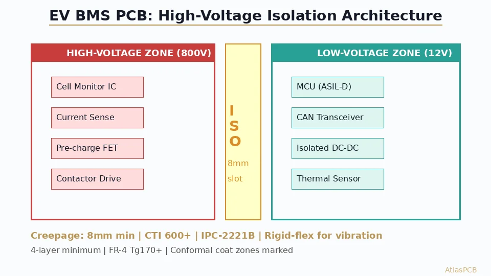
An 800V EV battery pack contains individual cells stacked in series, creating voltage potentials between the highest and lowest cells that exceed 800V during charging. The BMS PCB must simultaneously connect to cells at full pack voltage (through isolated monitoring ICs like the ADBMS6830 or MAX17852) and communicate with a low-voltage MCU running at 12V or 3.3V that interfaces to the vehicle CAN bus.
The isolation boundary between these domains is not merely an electrical requirement — it is a safety-critical feature that must survive throughout the vehicle lifetime (15 years, 300,000 km) including exposure to contamination, humidity, altitude, and vibration. IPC-2221B specifies creepage and clearance distances based on working voltage, pollution degree (how dirty the environment is), and the comparative tracking index (CTI) of the substrate material.
For 800V working voltage at pollution degree 2 (typical enclosed automotive electronics), IPC-2221B requires 8mm minimum creepage on material with CTI 400+. This 8mm distance must be maintained across the PCB surface between any conductor connected to the HV domain and any conductor connected to the LV domain. The practical implementation uses routed slots — completely removing PCB substrate material along the isolation boundary — to prevent surface tracking even if contamination bridges the gap.
In our facility, we route isolation slots using 2mm end mills with positional accuracy of +/-0.1mm. The slot edges are left unplated (no exposed copper) and solder mask extends to within 0.5mm of the slot edge to prevent moisture wicking along exposed glass fibers. For designs requiring conformal coating, we define coating boundaries that bridge the slot only where optically isolated communication (typically digital isolators or isolated gate drivers) crosses the boundary through the air gap above the slot.
PCB MANUFACTURER FOR AUTOMOTIVE
EV BMS PCBs with Certified Isolation
IPC-2221B compliant designs with hi-pot tested isolation slots. ISO 9001 quality system for automotive production.
Get BMS PCB Quote ›
Why Rigid-Flex Is Becoming Standard for BMS
Traditional BMS designs use rigid PCBs connected by wire harnesses or flexible flat cables (FFC) to cell monitoring daughter boards distributed throughout the battery pack. This architecture works for 400V systems with modest vibration requirements, but the industry shift to 800V platforms and larger battery packs has exposed fundamental reliability weaknesses in connector-based approaches.
The vibration environment inside an EV battery pack is unrelenting. Road surface irregularities create continuous excitation at 5-50 Hz with acceleration levels of 2-5G RMS. Board-to-board connectors — even automotive-grade units — experience fretting corrosion at contact points subjected to micro-motion. Our reliability data from returned field units shows connector-related intermittent failures beginning at 3,000-5,000 hours of operation, well within the 15-year vehicle lifetime target.
Rigid-flex construction eliminates every connector in the HV monitoring chain. The rigid sections carry the complex circuitry (MCU, isolated power supplies, CAN transceivers), while polyimide flex tails extend directly to each cell monitoring IC location. These flex sections are designed to absorb vibration and thermal expansion through controlled bend geometry, with the polyimide substrate surviving millions of flex cycles without fatigue when designed within its dynamic bend radius specifications.
The cost comparison has shifted decisively in favor of rigid-flex for 800V BMS. While the PCB itself costs 40-60% more than an equivalent rigid board, the total assembly cost drops by 25-35% due to eliminated connectors ($2-8 per connector position), eliminated harness assembly labor (15-30 minutes per battery module), and eliminated connector-related field failures (warranty cost reduction). For a typical 96-cell battery pack with 12 monitoring ICs, the connector elimination saves approximately $45-80 in BOM cost while adding $30-50 in PCB premium — with the reliability improvement being priceless in safety-critical automotive applications.
Thermal Management for Current Sensing
BMS PCBs carry significant currents — both the cell monitoring connections (typically 1-5A during balancing) and, in some architectures, the main pack current path through sense resistors mounted directly on the BMS board. Managing the thermal implications of these currents without affecting measurement accuracy requires careful PCB design.
Current sense resistors (shunt resistors) on BMS boards typically handle 50-200A of main pack current. A 0.5 milliohm sense resistor passing 200A dissipates 20W — concentrated in a component footprint of approximately 10x5mm. The PCB copper connecting to this component must handle the full current without exceeding acceptable temperature rise, while simultaneously providing a low-impedance kelvin connection for the sense amplifier.
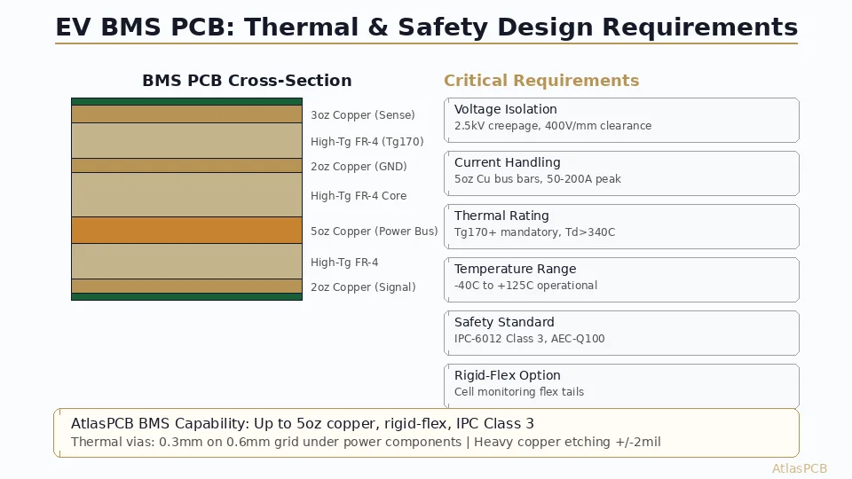
We recommend 3oz (105um) copper on layers connecting to current sense components, with thermal relief patterns that allow adequate heat spreading without introducing parasitic resistance in the measurement path. The kelvin sense traces — thin traces connecting to the voltage measurement inputs of the sense amplifier — must be routed on separate copper from the power traces, connected directly at the resistor pads to avoid including copper resistance in the measurement.
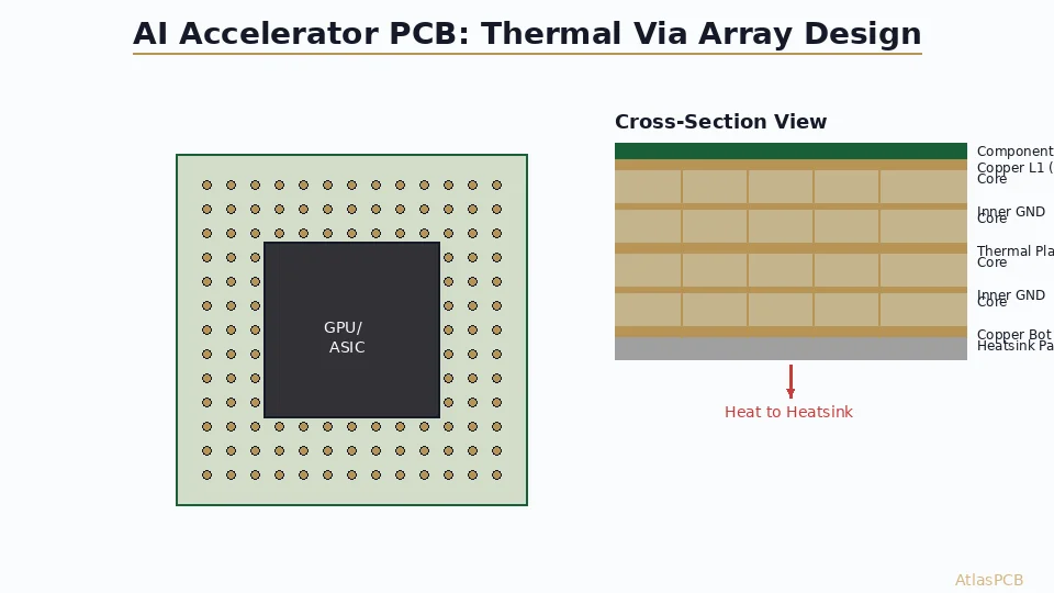
Thermal vias beneath high-dissipation components provide conductive paths to internal copper planes that act as heat spreaders. For a 20W dissipation in a 10x5mm footprint, we typically specify a grid of 0.3mm thermal vias on 1.0mm pitch, connecting the component mounting pad to at least two internal copper planes. This reduces the thermal resistance from component to board by approximately 40% compared to copper spreading alone, bringing the local temperature rise from 50-60C down to 25-35C above ambient.
The operating temperature consideration extends to material selection. Standard FR-4 (Tg 140) begins losing mechanical strength at 130C and is unsuitable for locations near high-current components or in areas exposed to pack thermal management system exhaust. FR-4 Tg170 provides adequate margin for most BMS applications, sustaining continuous operation at 130C without delamination risk. Polyimide substrates (Tg 260+) are reserved for flex sections and areas in direct thermal contact with cell busbars, where local temperatures can reach 140-150C during fast-charge events.
RIGID-FLEX PCB MANUFACTURER
Automotive-Grade Rigid-Flex for EV Applications
Up to 22-layer rigid-flex with 3oz copper, polyimide flex sections, and IPC-6013 Class 3 qualification for automotive reliability.
Request Rigid-Flex Quote ›Manufacturing Constraints Unique to BMS PCBs
Beyond the standard multilayer fabrication process, EV BMS boards impose several manufacturing requirements that elevate production complexity and cost:
Isolation slot routing must achieve clean edges without exposed glass fibers that could wick moisture and degrade surface insulation resistance over time. We use climb milling (a specific router bit engagement direction) to produce cleaner slot edges, followed by edge cleaning to remove any protruding glass fibers. The slot width is typically 2-3mm — wider than functionally necessary — to accommodate routing tool wear and provide margin for conformal coating application.
Heavy copper processing (2-3oz) on inner layers creates challenges during etching. Thick copper requires longer etch times, which widens the undercut beneath the resist and reduces achievable trace width. For 3oz copper, minimum trace/space increases from 3/3mil (75um) to approximately 5/5mil (125um). BMS designers must account for this constraint when routing high-current traces alongside fine-pitch IC breakouts on the same layer — often requiring two different copper weights on different layers within the same stackup.
Controlled impedance on boards with isolation slots requires careful attention to reference plane continuity. The isolation slot cuts through all layers of the board, removing both copper and dielectric material in the slot zone. Any controlled-impedance trace that approaches the slot will see its impedance increase as the reference plane disappears beneath it. We recommend keeping impedance-critical traces at least 5mm away from slot edges, or transitioning signals across the isolation boundary exclusively through optically-isolated communication ICs with their own local reference on each side.
Hi-pot (high-potential) testing is mandatory for every BMS board before shipment. We apply 1500-2000V DC between the HV and LV domains for 60 seconds, measuring leakage current. Acceptable leakage is below 1uA at rated voltage. This test catches fabrication defects that would not be visible in standard electrical testing — delamination within the slot region, copper slivers on slot walls, or contamination bridging the isolation gap. Boards that fail hi-pot are scrapped, contributing to the yield loss premium for BMS production.
IMPEDANCE CONTROLLED PCB MANUFACTURER
From BMS Prototype to Automotive Production
Hi-pot tested isolation, heavy copper inner layers, and rigid-flex construction — all qualified for automotive volume.
Design Checklist for EV BMS PCBs
Before submitting an EV BMS PCB design for quotation, verify these critical parameters:
Creepage and clearance distances meet IPC-2221B requirements for your working voltage, including accounting for altitude derating if the vehicle operates above 2000m (reduces air breakdown voltage). Isolation slots are dimensioned at minimum 2mm width with 0.5mm solder mask pullback from slot edges.
Copper weight is specified per layer — not as a blanket specification. High-current layers use 2-3oz while signal layers remain at 1oz or 0.5oz. The stackup must account for the different etch factors at each copper weight.
Rigid-flex transition zones are designed with proper stiffener coverage, adequate bend radius (minimum 6x material thickness for dynamic flex), and copper routing that follows flex guidelines — no vias within 1mm of the rigid-flex boundary, traces perpendicular to bend axis, and staggered (not symmetric) trace placement through the bend zone.
Thermal management features are specified including thermal via arrays under power components, defined no-copper keepout zones around temperature-sensitive measurements, and copper plane allocation for heat spreading.
Material specifications include Tg rating (minimum 170 for rigid sections), CTI value (minimum 400 for HV substrates, 600 preferred), and UL94 V-0 flammability rating. Flex sections specify polyimide type, adhesive system, and coverlay material.
Test requirements are documented including hi-pot voltage and duration, impedance test locations, and any thermal cycling qualification tests to be performed on production samples.
ATLASPCB
Building the Next Generation of EV Battery Electronics?
Upload your BMS design files and isolation requirements. Our automotive PCB engineers review creepage, thermal, and reliability constraints — returning a complete DFM report within 48 hours.
Submit BMS Design ›
Reviewed by AtlasPCB Engineering Team — 15+ years in advanced PCB fabrication for RF, HDI, and rigid-flex applications.
Related Reading:
About AtlasPCB — We specialize in complex PCB manufacturing for HDI, RF, and high-reliability applications. Explore our rigid-flex PCB manufacturing, or get an aluminum and metal-core PCB services . Every order includes free engineering review. Get your quote.
Reviewed by AtlasPCB Engineering Team — IPC-certified manufacturing specialists with 15+ years of production experience in HDI, RF, and high-reliability PCB fabrication. Content based on factory floor data and real customer design reviews.
Frequently Asked Questions
What creepage distance is required for 800V EV BMS PCBs?
Why use rigid-flex PCB for EV BMS instead of standard rigid boards with connectors?
What PCB material is best for EV BMS applications?
How thick should copper be for BMS current sensing traces?
- ev-pcb
- rigid-flex
- automotive
- thermal-management