· AtlasPCB Engineering · Engineering · 9 min read
AI Training Server PCB: 20+ Layer HDI Stackup Requirements for HBM Memory Channel Routing
A manufacturing-focused analysis of the PCB requirements for AI training server boards — covering 20-24 layer HDI stackups, HBM3/3e memory channel routing constraints, stacked microvia reliability, ultra-low-loss laminate selection, and the fabrication challenges that separate capable manufacturers from pretenders in the AI hardware supply chain.
Quick Answer
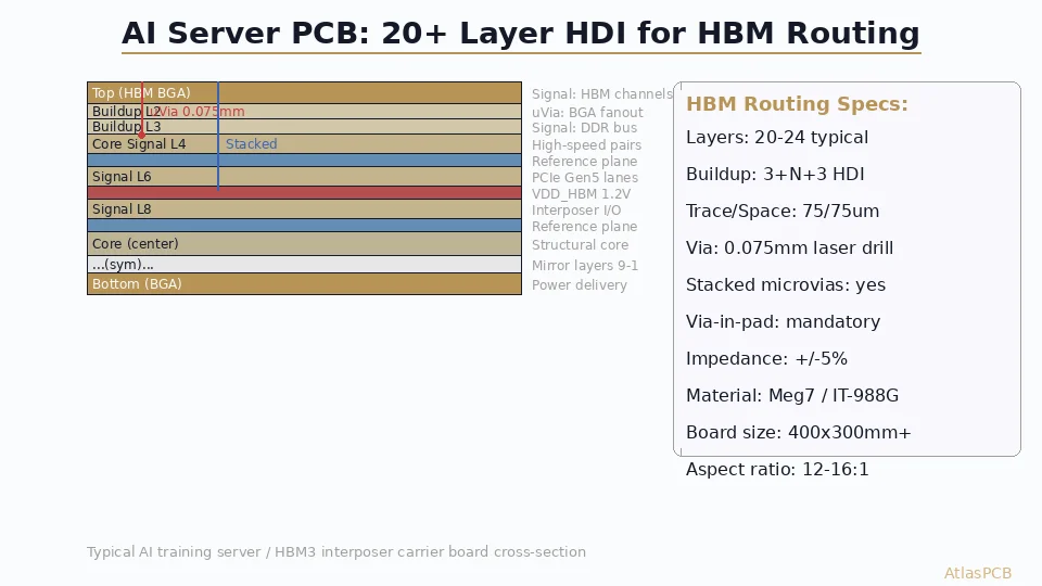
AI training server PCBs require 20-24 layer HDI construction with 3+N+3 or 4+N+4 buildup structures to route HBM3/3e memory channels at 9.6-12.8 Gbps per pin. The critical manufacturing requirements are: stacked microvias with copper-filled via-in-pad for BGA escape routing at 0.65-0.8mm pitch, ultra-low-loss laminates (Megtron 7, IT-988G SE, or equivalent with Df less than 0.002 at 10 GHz), 75/75um minimum trace/space, impedance control to +/-5%, and total board thickness management within 3.0-3.8mm to maintain structural rigidity across 400x300mm+ panel dimensions.
Quick Answer: AI Server PCB Manufacturing Requirements
| Parameter | AI Training Server Requirement | Standard Server PCB |
|---|---|---|
| Layer count | 20-24 (HDI) | 12-16 (through-hole) |
| HDI buildup | 3+N+3 or 4+N+4 | None or 1+N+1 |
| Laminate | Megtron 7, IT-988G SE (Df<0.002) | Standard FR-4 or low-loss FR-4 |
| Min trace/space | 75/75 um (3/3 mil) | 100/100 um (4/4 mil) |
| Via technology | Stacked microvias, VIPPO, via-in-pad | Through-hole, some blind |
| Laser drill | 0.075mm microvias | Not required |
| Aspect ratio | 12-16:1 | 8-10:1 |
| Board size | 400x300mm to 500x400mm | 300x250mm typical |
| Impedance control | +/-5% on 20+ controlled layers | +/-10% on 6-8 layers |
| Total thickness | 3.0-3.8mm | 1.6-2.4mm |
The AI hardware revolution has created a new tier of PCB manufacturing complexity that separates the industry into “can build AI server boards” and “cannot.”
Why AI Training Boards Push PCB Manufacturing to the Limit
The current generation of AI training accelerators — whether NVIDIA H100/B200, AMD MI300X, or custom ASICs — shares a common architectural pattern that drives extreme PCB requirements. Each accelerator package connects to multiple HBM (High Bandwidth Memory) stacks through a silicon interposer or advanced packaging substrate. The system board that carries these packages must route massive parallel bus widths (1024+ signals per HBM stack, typically 4-8 stacks per accelerator) at data rates of 9.6-12.8 Gbps per pin.
This combination of signal count, signal speed, and package density creates a routing challenge that simply cannot be solved on conventional through-hole PCBs. The math is straightforward: an HBM3 stack with a 0.65mm pitch BGA needs approximately 32x32 = 1024 balls in a roughly 21mm x 21mm footprint. Escaping all signals from this density requires routing channels at 75um trace with 75um spacing — and multiple layers of sequential buildup to fan out from the center of the array.
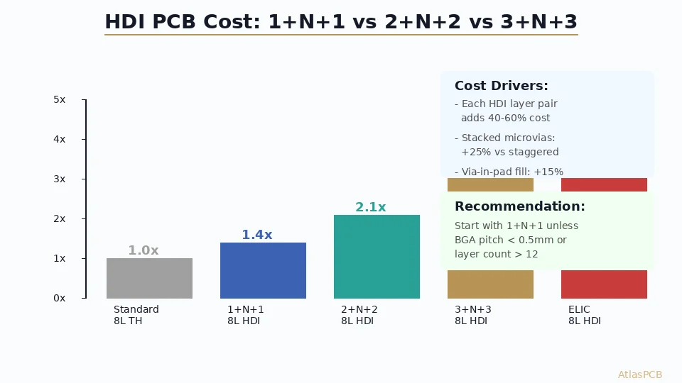
From a manufacturing perspective, this translates to very specific requirements that we encounter daily in AI hardware PCB production. The boards demand 3+N+3 or 4+N+4 HDI buildup — meaning three to four sequential lamination, drill, and plate cycles on each side of the core before the complete stackup is assembled. Each cycle adds roughly 2 days to fabrication time and introduces registration accuracy requirements that compound with each additional buildup layer.
Our process engineering team has observed that the reject rate on 22+ layer HDI boards is fundamentally higher than standard PCB production. Where a standard 8-layer FR-4 board might have a 98% first-pass yield, a 22-layer HDI on Megtron 7 with stacked microvias typically yields 85-92% even with mature processes. The yield loss comes primarily from microvia reliability (stacked via cracking during thermal cycling) and layer-to-layer registration drift across 10+ sequential process cycles.
HDI PCB MANUFACTURING
Up to 30 Layers, 5+N+5 HDI Buildup
Stacked microvias, VIPPO via-in-pad, sequential lamination. We manufacture HDI boards for AI accelerator platforms, HPC networking, and high-density computing applications.
View HDI Capabilities ›
Laminate Selection: Why Ultra-Low-Loss Is Non-Negotiable
The dielectric material choice for AI server PCBs is driven by a single metric: insertion loss budget at the HBM/SerDes data rate. An HBM3 channel running at 9.6 Gbps has a fundamental frequency around 4.8 GHz, with meaningful spectral content to the third harmonic (14.4 GHz). The total insertion loss from transmitter pad to receiver pad — including trace loss, via transitions, connector loss, and package escape — must stay within the receiver’s eye-opening budget.
On standard FR-4 (loss tangent 0.02 at 1 GHz, rising to 0.025+ at 10 GHz), a 50mm trace at 10 GHz loses approximately 1.5-2.0 dB per inch. For a 75mm HBM channel trace, that is 6-8 dB of trace loss alone — leaving virtually no margin for via transitions and package parasitics. The system simply does not work.
Ultra-low-loss laminates solve this by reducing the loss tangent by 10-20x. Panasonic Megtron 7 (Df = 0.001 at 12 GHz) delivers approximately 0.15-0.2 dB/inch at 10 GHz — a dramatic improvement that opens sufficient loss budget for the complete channel including four via transitions (transmitter escape, interposer transition, motherboard routing, receiver landing).
The material hierarchy for AI server boards in 2026:
| Material | Df @ 10 GHz | Dk | Typical Use | Relative Cost |
|---|---|---|---|---|
| Panasonic Megtron 7 | 0.001 | 3.3 | HBM channels, NVLink | 5x FR-4 |
| TUC IT-988G SE | 0.0015 | 3.3 | HBM routing, PCIe Gen5 | 4x FR-4 |
| Isola I-Tera MT40 | 0.0028 | 3.45 | PCIe Gen5, general high-speed | 3x FR-4 |
| Panasonic Megtron 6 | 0.003 | 3.4 | Previous-gen servers, networking | 2.5x FR-4 |
| Standard low-loss FR-4 | 0.008-0.012 | 4.2 | DDR5, moderate high-speed | 1.5x FR-4 |
| Standard FR-4 | 0.02 | 4.5 | Industrial, low-speed digital | 1x (baseline) |
Material selection interacts with manufacturing in important ways. Megtron 7 and IT-988G SE have different drilling characteristics than FR-4 — they are cleaner to drill (less smear) but require different desmear chemistry. Their lamination profiles differ (lower Tg materials require lower press temperatures with longer dwell times). And critically, their in-plane CTE characteristics are different, which affects layer-to-layer registration accuracy during sequential lamination of 20+ layer stacks.
Stacked Microvias: The Critical Manufacturing Challenge
Stacked microvias are the enabling technology for HBM BGA escape routing, and simultaneously the primary yield-limiting process step in AI server PCB manufacturing. A stacked microvia structure involves drilling a 0.075-0.1mm laser via in one buildup layer, copper-filling it completely (not just plating the walls), planarizing the surface flat, and then drilling another via directly on top of the filled via in the next buildup layer.
The reliability concern is well-documented in IPC literature and thermal cycling data: when a stacked microvia column (3-4 levels deep) experiences thermal cycling between -40C and +125C, differential CTE between the copper fill and the surrounding dielectric creates stress at the via-to-via interface. If the copper fill contains any voids, the thermal stress concentrates at those defects and initiates a crack that propagates through the interface — creating an open circuit.
Manufacturing stacked microvias reliably requires precise control of several parameters that we monitor in our HDI production line. The copper fill process (DC plating with specific additive chemistry) must achieve greater than 95% fill density — any void larger than 5-10um becomes a potential crack initiation site. The planarization step (surface grinding to remove copper bumps above filled vias) must achieve flatness within +/-5um to ensure the subsequent buildup layer adheres uniformly. And the laser drilling of the next-level via must be precisely aligned to the filled via below — registration accuracy must be within +/-15um to ensure the drill lands entirely within the copper fill without hitting the surrounding dielectric edge.
We qualify our stacked microvia process with IST (Interconnect Stress Testing) per IPC-TM-650 2.6.26, cycling between 23C and 150C for 1000+ cycles with continuous resistance monitoring. A properly manufactured 3-stack microvia shows less than 5% resistance increase after 1000 thermal cycles. A defective structure (insufficient fill, voids, misregistration) typically fails within 100-200 cycles.
STACKED MICROVIA RELIABILITY
IST-Qualified Process for AI Hardware
Our stacked microvia process is qualified to 1000+ thermal cycles (23-150C) per IPC-TM-650. Copper fill density >95%, registration +/-15um, planarization +/-5um.
View Process Data ›Power Delivery: The Hidden Layer Count Driver
While the signal routing requirements of HBM channels are the most technically demanding aspect, the power delivery network (PDN) is often what pushes AI server boards from 16 to 20+ layers. A modern AI accelerator consuming 300-700W at 0.7-0.85V core voltage requires enormous plane copper area to maintain PDN impedance below the target (typically less than 0.5 milliohms from VRM to die).
The PDN of a 700W accelerator at 0.8V draws approximately 875A peak current. Delivering this through PCB planes without excessive voltage droop requires multiple dedicated power/ground plane pairs — typically 3-4 power planes and 4-5 ground planes in a 22-layer stack. Each power domain (VDD_CORE, VDD_HBM, VDD_IO, VDD_PLL) needs its own plane to prevent cross-coupling between high-current core supply and sensitive analog supplies.
From a manufacturing perspective, these power planes require 2oz (70um) or even 3oz (105um) copper weight — significantly thicker than the 0.5oz (17.5um) or 1oz (35um) used for signal layers. The combination of thick copper planes with thin signal layers creates asymmetric stress in the stackup during lamination, which can cause warpage in large-format boards (400x300mm+). Our stack-up engineering team designs symmetric copper distribution (equal total copper weight above and below the center) to minimize warpage while meeting both PDN impedance and signal integrity requirements.
Manufacturing Qualification: What to Ask Your HDI Fabricator
If you are designing or sourcing AI training server PCBs, the manufacturer qualification process should verify capabilities that standard PCB shops simply do not have. Here is what we recommend verifying — and what we provide to customers evaluating our facility for AI hardware production:
1. Sequential lamination count — how many buildup cycles can they reliably execute? AI server boards need 3+N+3 minimum (6 sequential cycles). Ask for yield data on 3+N+3 and 4+N+4 builds.
2. Stacked microvia reliability data — request IST or thermal cycling test results specifically for their stacked microvia process. Acceptable: 1000+ cycles at 23-150C with less than 5% resistance change. Unacceptable: “we haven’t tested it.”
3. Ultra-low-loss material experience — have they processed Megtron 7 or equivalent? These materials require different press profiles, desmear chemistry, and surface preparation. A fabricator experienced with Megtron 6 may need process development time for Megtron 7.
4. Registration accuracy across 20+ layers — what is their layer-to-layer registration capability on sequential buildup structures? Target: +/-25um or better between any two layers.
5. Via-in-pad fill and planarization — can they achieve >95% fill density with +/-5um surface planarity? Ask for cross-section photos of filled vias from recent production.
6. Large-format capability — AI server boards are physically large (400x300mm to 500x400mm). Not all HDI fabricators can maintain process control across these dimensions. Warpage must stay within 0.75% per IPC-6012 Class 3.
ATLASPCB
Building AI Hardware? Let Us Review Your HDI Requirements
Up to 30 layers, 5+N+5 HDI buildup, stacked microvias, ultra-low-loss materials. We manufacture HDI boards for AI accelerator platforms with IST-qualified processes. Upload your stackup for a manufacturability assessment.
Upload Design ›
Reviewed by AtlasPCB Engineering Team — 15+ years in advanced PCB fabrication for RF, HDI, and rigid-flex applications.
Related Reading:
About AtlasPCB — We specialize in complex PCB manufacturing for HDI, RF, and high-reliability applications. Explore our HDI PCB manufacturing capabilities, RF and high-frequency PCB services, or get an impedance-controlled PCB manufacturing . Every order includes free engineering review. Get your quote.
Reviewed by AtlasPCB Engineering Team — IPC-certified manufacturing specialists with 15+ years of production experience in HDI, RF, and high-reliability PCB fabrication. Content based on factory floor data and real customer design reviews.
Frequently Asked Questions
How many layers does an AI server PCB typically require?
What laminate materials are used for AI server PCBs?
What HDI buildup is needed for HBM BGA fanout?
Can a standard PCB manufacturer build AI server boards?
What does a 22-layer HDI AI server PCB cost?
- HDI PCB manufacturer
- PCB stackup design guide
- multilayer PCB cost
- RF PCB design and manufacturing
- impedance controlled PCB manufacturer