· AtlasPCB Engineering · Engineering · 10 min read
5G Antenna PCB Fabrication: Via Fencing, Cavity-Backed Design, and Material Considerations for 28 GHz Phased Arrays
Engineering-grade manufacturing guide for 5G mmWave antenna PCBs. Covers via fencing pitch calculation, cavity-backed patch antenna construction, Rogers material bonding, and the critical fabrication tolerances that determine whether your 28 GHz array achieves specification or radiates a defocused pattern.
Quick Answer
28 GHz phased array antenna PCBs require via fencing at lambda/10 pitch (approximately 1.1mm on Rogers 4350B) to prevent surface wave coupling between elements, with via diameter of 0.2-0.3mm and clearance of 0.15mm minimum from antenna element edges. The critical fabrication tolerance is via position accuracy — at 28 GHz, a 50um via placement error shifts null depth by 3-5 dB in a 16-element array. Manufacturing this requires drill registration better than +/-25um and Rogers material laminated on dedicated presses with verified CTE matching.
Quick Reference: 28 GHz Phased Array PCB Manufacturing Requirements
| Parameter | Requirement | Why It Matters |
|---|---|---|
| Material | Rogers 4350B or RO3003 | Dk stability at mmWave, low Df |
| Via fence pitch | 0.5mm (max 0.57mm) | Surface wave isolation |
| Via diameter | 0.2-0.3mm | Fits 0.5mm pitch with clearance |
| Via position accuracy | +/-25um | Phase error < 0.5 degree/element |
| Dk tolerance | +/-2% (board level) | Element resonance frequency control |
| Surface finish (antenna) | Immersion Ag or OSP | Avoids nickel RF loss |
| Copper roughness (Rz) | < 1.5um | Conductor loss at 28 GHz |
| Lamination registration | +/-25um layer-to-layer | Feed network alignment |
Why 28 GHz Changes Everything About PCB Antenna Fabrication
At sub-6 GHz frequencies — where most 4G and WiFi antennas operate — PCB fabrication tolerances are generous relative to wavelength. A 50um position error on a 3.5 GHz antenna element represents less than 0.2% of a wavelength, creating negligible phase error. The antenna works even with standard PCB manufacturing tolerances.
At 28 GHz, the same 50um error represents 0.5% of the free-space wavelength (10.7mm) — small in absolute terms but significant in a phased array context where errors compound across elements. A 16-element linear array with random 50um position errors across all elements degrades beam pointing accuracy by approximately 0.3 degrees and sidelobe level by 2-3 dB. For a 64-element planar array, these errors become the dominant factor limiting achievable sidelobe suppression.
The fabrication challenge is further compounded by the material behavior at mmWave frequencies. Rogers 4350B Dk stability of +/-1.5% translates to +/-1.5% variation in guided wavelength — at 28 GHz, this means patch resonant frequency varies by +/-420 MHz across the panel. For a patch antenna with 3-5% bandwidth, this panel-level Dk variation can shift individual elements to the edge of their operating bandwidth, degrading gain by 1-2 dB at band edges.
In our facility, we address this by measuring Dk on test coupons from each Rogers panel before processing production boards. Panels with Dk outside +/-1% of target (tighter than Rogers’ datasheet specification) are rejected or assigned to less demanding applications. This incoming material screening adds approximately $1-2 per board to cost but eliminates the largest source of systematic antenna performance variation.
MMWAVE RF EXPERTISE
28 GHz Antenna PCBs With Verified Registration
We measure and report drill registration accuracy on every mmWave antenna panel. X-ray verification included at no extra charge for phased array builds.
Get RF Quote ›
Via Fencing Design: The Math Behind Isolation
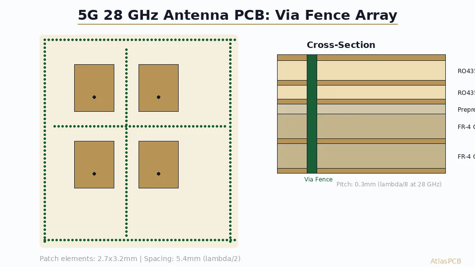
Via fencing prevents surface wave propagation between antenna elements by creating an electromagnetic boundary condition. The physics is analogous to a waveguide below cutoff — when the via-to-via spacing is less than lambda/2, no propagating mode can exist between adjacent vias, effectively creating a metallic wall.
For maximum isolation, the via pitch must satisfy two conditions: the gap between via walls (pitch minus diameter) must be less than lambda_g/2 to prevent propagation, and the via must extend through the full substrate thickness to prevent leakage below the fence. At 28 GHz on Rogers 4350B:
- Guided wavelength: lambda_g = c / (f * sqrt(Dk_eff)) = 10.7mm / sqrt(3.48) = 5.74mm
- Maximum via gap for cutoff: lambda_g / 2 = 2.87mm
- Recommended pitch for 20+ dB isolation: lambda_g / 10 = 0.57mm
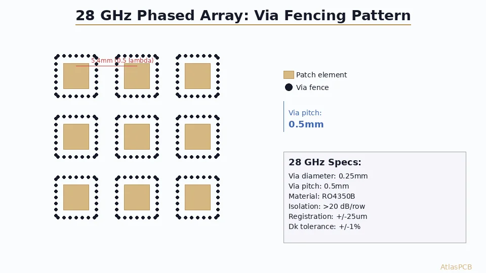
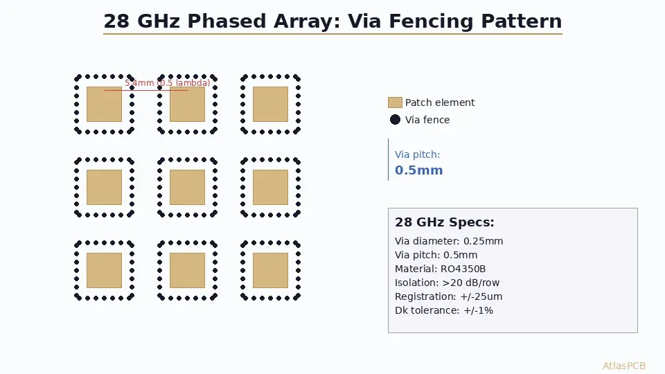
- Practical pitch allowing 0.25mm via + 0.32mm web: 0.5mm center-to-center
Each row of via fencing provides approximately 15-20 dB of surface wave isolation at 28 GHz. Two rows (inner at 0.5mm pitch, outer at 0.8mm) provide 30-35 dB — sufficient for most phased array applications where element-to-element coupling below -20 dB is required.
From a manufacturing standpoint, 0.5mm-pitch vias at 0.25mm diameter are straightforward with mechanical drilling. The challenge is maintaining position accuracy across a panel with hundreds of fence vias per element. Our CNC drill platforms achieve +/-25um position accuracy using laser-measured tooling hole references, which keeps fence-to-element distance consistent to within +/-50um across a full 18x24-inch production panel.
Cavity-Backed Antenna Construction: Step-by-Step Fabrication
The cavity-backed patch antenna is the dominant architecture for 28 GHz phased arrays because it provides element isolation without physical separation — enabling half-wavelength element spacing (5.4mm) that maximizes scan range. The cavity is formed entirely by via fencing, requiring no milling, routing, or exotic construction.
Manufacturing sequence for a cavity-backed 28 GHz array:
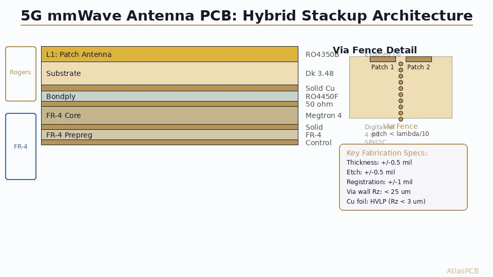
The core layer (Rogers 4350B, 0.254mm/10mil thickness) serves as the antenna substrate. Patch elements are etched on the top surface; the ground plane is on the bottom. Via fences are drilled through the full core thickness, connecting the top ground pour surrounding each patch to the bottom ground plane. The via diameter is 0.25mm with 0.15mm annular ring on each side, placed at 0.5mm pitch in a rectangular pattern surrounding each element.
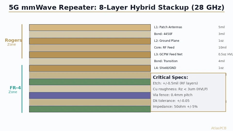
Feed network layers (if using aperture coupling) are built below the ground plane using additional Rogers or FR-4 layers bonded with Rogers 4450F prepreg. The coupling slot in the ground plane must align with the patch element above to within +/-25um — this registration is the most critical alignment in the entire build.
In our production line, we achieve this through a combination of techniques: X-ray drill targeting for innerlayer registration, optical alignment for outer layer imaging, and post-lamination X-ray measurement to verify achieved registration before proceeding to outer layer processing. Panels that exceed +/-30um registration are reworked or rejected at this stage rather than completing processing that would result in functional failure.
PHASED ARRAY MANUFACTURING
Production-Ready Phased Array Antenna PCBs
From 4-element evaluation boards to 256-element production arrays. We handle Rogers material procurement, via fencing optimization, and full X-ray registration verification.
Material Selection: Rogers Family Comparison for 28 GHz
Not all Rogers materials are equal at mmWave frequencies. The choice depends on your array size, thermal requirements, and budget:
| Material | Dk (28 GHz) | Df (28 GHz) | Thermal Cond. | FR-4 Process Compatible | Cost Index |
|---|---|---|---|---|---|
| RO4350B | 3.48 | 0.0050 | 0.69 W/mK | Yes | 1.0x |
| RO4835 | 3.48 | 0.0040 | 0.62 W/mK | Yes | 1.3x |
| RO3003 | 3.00 | 0.0013 | 0.50 W/mK | No (PTFE handling) | 2.2x |
| RT/duroid 5880 | 2.20 | 0.0009 | 0.20 W/mK | No (PTFE handling) | 2.8x |
| TMM10i | 9.80 | 0.0020 | 0.76 W/mK | Yes (thermoset) | 1.8x |
For 28 GHz phased arrays with 16-64 elements, Rogers 4350B is the default choice. Its FR-4 process compatibility means standard oxide treatment, standard drill speeds, and standard solder mask adhesion — no special handling premiums. The Df of 0.005 at 28 GHz adds approximately 0.3 dB of dielectric loss per wavelength of feed network length, which is acceptable for most commercial 5G applications.
For arrays exceeding 64 elements where cumulative feed network loss becomes a system bottleneck, RO3003 reduces dielectric loss by 3-4x. However, its PTFE base requires plasma surface treatment for adhesion (adding $2-3/board), specialized drill parameters (30% slower feed rate), and plasma-cleaned surfaces before plating. These process premiums add 40-60% to fabrication cost above the already-higher material cost.
From our experience fabricating 5G antenna arrays for base station OEMs, RO4350B satisfies requirements for all small cell and CPE antenna applications up to 64 elements. RO3003 becomes necessary primarily for active antenna unit (AAU) designs with 128+ elements where the corporate feed network exceeds 8 wavelengths in length.
Surface Finish Impact on Antenna Efficiency at 28 GHz
Surface finish selection directly impacts antenna radiation efficiency because skin depth at 28 GHz is approximately 0.4um in copper — meaning the first few hundred nanometers of conductor surface carry essentially all the RF current. Any lossy material in this skin-depth region degrades efficiency.
ENIG (Electroless Nickel Immersion Gold) deposits 3-5um of nickel before the gold layer. Nickel is ferromagnetic with much higher resistivity (69.3 nΩ·m) compared to copper (16.8 nΩ·m). At 28 GHz, the nickel layer is approximately 10x skin depth thick — completely dominating the surface current path. Measured antenna efficiency with ENIG is consistently 0.7-1.2 dB worse than bare copper at 28 GHz.
Immersion silver (0.15-0.3um) provides excellent surface conductivity (only marginally higher resistivity than copper) without a lossy barrier layer. It maintains antenna efficiency within 0.1-0.2 dB of bare copper and provides adequate shelf life for assembly (6-12 months with proper storage).
Our recommended approach for phased array boards: selective surface finish. Antenna radiating elements and feed network traces receive immersion silver; component pads, connector footprints, and BGA lands receive ENIG for reliable soldering. This requires two surface finish processes (additional cost of $1-2/board) but optimizes both RF performance and assembly reliability.
SELECTIVE SURFACE FINISH
Dual Surface Finish for Antenna + Assembly
We offer selective ENIG/Immersion Silver processing — optimize RF performance on antenna elements while maintaining ENIG solderability on component pads.
See Our Capabilities ›Production Yield and Quality Assurance for mmWave Antenna Boards
28 GHz antenna PCBs have tighter pass/fail criteria than standard impedance-controlled boards because antenna performance is binary — either the element resonates at the target frequency with acceptable gain, or it does not, and there is no rework path for a printed antenna that is off-frequency.
Our quality assurance process for phased array PCBs includes:
First-article verification involves test coupon measurements of Dk (ring resonator method, measured at 28 GHz), impedance (TDR on feed network test structures), and registration (X-ray measurement of via-to-pad alignment). Production release requires all three measurements within specification.
In-process inspection adds panel-level registration measurement after each drilling step, with automatic rejection of panels exceeding +/-30um. This catches registration drift from temperature variation or drill wear before additional processing is invested in a defective panel.
Final inspection includes 100% visual inspection of antenna element geometry (etch uniformity, no copper remnants in gaps) using automated optical inspection (AOI) calibrated for the specific pad geometry. For critical applications, we add electrical test of antenna element isolation using a bed-of-nails fixture that contacts each element feed point and measures S21 between adjacent elements.
Typical production yield for 28 GHz phased array boards in our facility is 92-95% at the panel level — meaning 5-8% of panels require repair or replacement. The primary rejection causes are via registration out of spec (3-4%), Rogers material Dk out of range (1-2%), and etch defects on antenna elements (1-2%). These yield numbers assume proper incoming material screening and process control; without Dk verification, material-related yield loss can reach 5-8% alone.
ATLASPCB
Building a 5G Phased Array? Start With the Right PCB Partner.
Upload your antenna array design for a detailed manufacturing assessment. We evaluate registration requirements, recommend material options, and provide yield estimates based on your specific element count and frequency.
Get Manufacturing Assessment ›
Reviewed by AtlasPCB Engineering Team — 15+ years in advanced PCB fabrication for RF, HDI, and rigid-flex applications.
Related Reading:
About AtlasPCB — We specialize in complex PCB manufacturing for HDI, RF, and high-reliability applications. Explore our RF and high-frequency PCB services, Rogers RO4350B PCB manufacturing, or get an impedance-controlled PCB manufacturing . Every order includes free engineering review. Get your quote.
Reviewed by AtlasPCB Engineering Team — IPC-certified manufacturing specialists with 15+ years of production experience in HDI, RF, and high-reliability PCB fabrication. Content based on factory floor data and real customer design reviews.
Frequently Asked Questions
What via pitch is required for 28 GHz antenna PCB isolation?
Can Rogers 4350B handle 28 GHz antenna fabrication reliably?
What fabrication tolerance matters most for phased array PCBs?
How does cavity-backed construction improve 28 GHz antenna performance?
What surface finish is best for 28 GHz antenna PCBs?
- 5G antenna PCB fabrication
- RF PCB design and manufacturing
- Rogers 4350B stackup
- China RF PCB manufacturer
- impedance controlled PCB manufacturer