· AtlasPCB Engineering · News · 8 min read
ViaCore to Launch World's First Direct-Plating Glass Substrate Pilot Line in October 2026
Korean startup ViaCore will begin operating the world's first glass substrate pilot line using direct-plating technology in October 2026, eliminating the need for expensive sputtering chambers and potentially accelerating glass substrate adoption for AI chip packaging and advanced interposers.

Korean glass substrate technology company ViaCore has announced that it will begin operating the world’s first glass substrate pilot line using a proprietary direct-plating process at its facility in Ansan, Gyeonggi Province, in October 2026. The startup plans to complete performance testing of its mass-production equipment by mid-September before bringing both lines into active operation, marking a significant milestone in the global race to commercialize glass substrates for advanced semiconductor packaging.
The announcement positions ViaCore as the first company anywhere in the world to operate a pilot-scale glass substrate line that bypasses conventional sputtering entirely, instead using a chemical metallization approach that bonds copper directly to the glass surface. If the technology performs as promised at scale, it could fundamentally reshape the economics of glass substrate manufacturing and accelerate adoption timelines across the AI chip packaging ecosystem.
Direct Plating vs. Sputtering: A Paradigm Shift in Glass Metallization
The conventional approach to metallizing glass substrates relies on physical vapor deposition (PVD), commonly known as sputtering. In this process, a thin seed layer of metal is deposited onto the glass surface inside a vacuum chamber by bombarding a metal target with ionized gas. The sputtered atoms travel across the chamber and coat the substrate, creating an adhesion layer upon which subsequent copper plating can build.
While sputtering is a well-established technique borrowed from semiconductor front-end manufacturing, it carries significant drawbacks when applied to glass substrates. A single sputtering chamber capable of handling large-format glass panels costs approximately $6.6 million USD. The process is inherently batch-limited, energy-intensive, and requires precise vacuum conditions that increase both capital expenditure and cycle time. Furthermore, sputtering equipment is typically optimized for specific glass types and thicknesses, reducing manufacturing flexibility.
ViaCore’s direct-plating process eliminates the sputtering step entirely. Instead of relying on PVD to create an initial metal seed layer, the company’s proprietary technology uses a specialized layer structure that achieves chemical bonding between the metal and the glass surface. The process incorporates stress-relief mechanisms at the glass-metal interface, addressing one of the critical challenges in glass substrate manufacturing: the coefficient of thermal expansion (CTE) mismatch between glass and copper that can cause delamination during thermal cycling.
The practical implications are substantial. By removing the need for multi-million-dollar sputtering chambers, ViaCore’s approach dramatically lowers the capital barrier to glass substrate production. Perhaps more importantly, the direct-plating process works with different types and suppliers of glass, offering manufacturing flexibility that sputtering-based approaches cannot easily match. This glass-agnostic capability means fabricators are not locked into a single glass supplier or formulation, a meaningful advantage as the industry is still converging on optimal glass compositions for different applications.
Pilot Line Configuration and Production Roadmap
ViaCore’s Ansan facility will house two distinct pilot lines, each targeting different aspects of the glass substrate development pipeline. The first line handles 240x240mm substrates and serves primarily as a production validation platform. Its purpose is to prove process control, yield, and reliability at a format that can be directly scaled to the 510x515mm panel size that the industry has converged on for high-volume manufacturing.
The second line processes 120x120mm substrates and is dedicated to research and development activities. This smaller-format line will be used to explore new materials, optimize through-glass via (TGV) integration, develop cavity structures for embedded components, and test novel hole designs. Both lines target the two primary glass substrate product categories: glass core substrates (GCS) and glass interposers.
The roadmap beyond October 2026 is aggressive. ViaCore plans to have a full 510x515mm production line operational by the end of Q2 2027, less than nine months after pilot line commissioning. This timeline, if achieved, would place ViaCore among the first companies globally to offer production-scale glass substrates, competing directly with significantly larger players that have been developing glass substrate capabilities for years.
The Glass Substrate Race: Industry Context
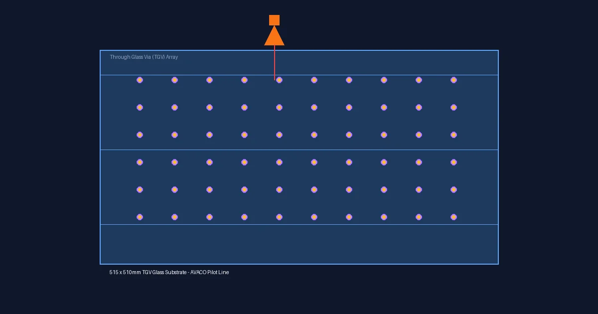
ViaCore’s announcement arrives amid intensifying competition in glass substrate development, particularly among Korean companies. Earlier this year, AVACO announced its own glass substrate pilot line focused on TGV processing equipment, while equipment maker Taesung has been developing specialized glass handling and processing tools for the substrate industry. Korean government-backed initiatives have also accelerated, with multiple consortiums forming to establish domestic glass substrate supply chains.
Globally, the glass substrate race is being driven by the insatiable demand for more advanced packaging solutions to serve AI accelerators and high-bandwidth memory. Intel has been the most vocal among major chipmakers about its glass substrate ambitions, publicly committing to glass substrate adoption in its advanced packaging roadmap and operating development lines at its facilities in Arizona. Samsung’s semiconductor division has similarly invested in glass substrate R&D, recognizing that organic substrates are approaching their physical limits for the wiring density and flatness requirements of next-generation chip packages.
TSMC, while less public about specific glass substrate timelines, has acknowledged the technology as part of its advanced packaging evolution beyond current CoWoS and InFO platforms. The foundry giant’s enormous production volumes mean that any glass substrate transition, even partial, would represent massive demand for glass substrate suppliers.
China has also entered the race aggressively, with multiple state-backed initiatives and newly formed industry alliances targeting glass substrate development. The strategic importance of advanced packaging for AI chip production has elevated glass substrates from a research curiosity to a supply-chain priority across all major semiconductor manufacturing regions.
Need Advanced Substrate or HDI PCBs?
While glass substrates are still in pilot production, AtlasPCB manufactures HDI boards with microvias, any-layer interconnects, and advanced substrate-like features for current-generation designs. Get engineering support from our team.
Request an HDI QuoteImpact on PCB and Advanced Packaging Industries
The emergence of viable glass substrate manufacturing has profound implications for the broader PCB and packaging industry. Glass core substrates offer several fundamental advantages over traditional organic substrates: near-zero warpage due to the dimensional stability of glass, significantly finer line and space capabilities enabled by the ultra-smooth glass surface, and superior thermal stability that allows tighter process windows during assembly.
For the interposer market specifically, glass substrates offer a compelling middle ground between expensive silicon interposers (used in current high-end AI packages) and organic substrates that cannot achieve the required wiring density. A glass interposer can deliver silicon-like routing density at a fraction of the cost, potentially enabling wider adoption of chiplet-based architectures beyond just the highest-end AI accelerators.
ViaCore’s direct-plating innovation adds another dimension to this value proposition. By eliminating the most capital-intensive step in glass substrate fabrication, the technology could bring glass substrate pricing closer to the range where it becomes viable for applications beyond cutting-edge AI chips. High-performance networking ASICs, advanced automotive processors, and next-generation mobile SoCs could all potentially benefit from glass substrates if manufacturing costs continue to decline.
The PCB industry supply chain is also watching closely. As glass substrates capture the most demanding applications currently served by advanced HDI and substrate-like PCBs, fabricators will need to evolve their capabilities accordingly. Companies with expertise in HDI manufacturing with microvias and fine-line processing are best positioned to understand and eventually adopt glass substrate techniques, as many of the downstream processes (pattern plating, lamination, routing) share fundamental similarities.
What This Means for Hardware Engineers Today
For engineers currently designing products and selecting PCB technologies, the glass substrate transition remains a near-future event rather than a present-day option. Pilot lines like ViaCore’s are proving the technology, but production-qualified glass substrates for commercial designs are likely still 18-24 months away for most applications, and initially limited to the highest-volume, highest-performance segments.
However, the trajectory is clear. Hardware engineers designing next-generation platforms should begin considering how glass substrates might affect their packaging roadmaps, particularly for designs requiring ultra-fine pitch interconnects, large interposer sizes, or extreme flatness for advanced assembly processes. Understanding TGV design rules and glass substrate stackup conventions now will provide a head start when the technology becomes commercially available.
In the meantime, the advanced HDI and substrate-like PCB technologies available today continue to serve the vast majority of high-performance applications effectively. Any-layer HDI with stacked microvias, semi-additive processing (SAP) for fine lines, and embedded component technologies all push the boundaries of what organic PCBs can achieve, bridging the gap until glass substrates reach full commercial maturity.
Need Advanced Substrate or HDI PCBs?
While glass substrates are still in pilot production, AtlasPCB manufactures HDI boards with microvias, any-layer interconnects, and advanced substrate-like features for current-generation designs. Get engineering support from our team.
Request an HDI QuoteViaCore’s direct-plating breakthrough represents exactly the kind of manufacturing innovation that could accelerate the glass substrate timeline for the entire industry. By proving that high-quality glass metallization is achievable without the capital burden of sputtering equipment, the company is lowering the barrier to entry for glass substrate fabrication globally. Whether ViaCore itself becomes a major volume producer or licenses its technology to established substrate manufacturers, the ripple effects of this pilot line’s success will be felt across the semiconductor packaging supply chain for years to come.
Sources: ETNews Korea, ic-pcb.com
About AtlasPCB — We specialize in complex PCB manufacturing for HDI, RF, and high-reliability applications. Explore our impedance-controlled PCB manufacturing . Every order includes free engineering review. Get your quote.
Reviewed by AtlasPCB Engineering Team — IPC-certified manufacturing specialists with 15+ years of production experience in HDI, RF, and high-reliability PCB fabrication. Content based on factory floor data and real customer design reviews.
- glass substrate
- advanced packaging
- TGV
- interposer
- semiconductor packaging
- AI chips
- ViaCore
- direct plating