· AtlasPCB Engineering Team · News · 5 min read
AVACO Launches 515x510mm TGV Glass Substrate Pilot Line, Accelerating Next-Generation Semiconductor Packaging
Korean equipment manufacturer AVACO has started operating a 515x510mm TGV glass substrate pilot line in partnership with AVATEC, targeting mass-production samples by end of 2026 and metallized substrates from 2027 as the industry races toward glass-based advanced packaging solutions.
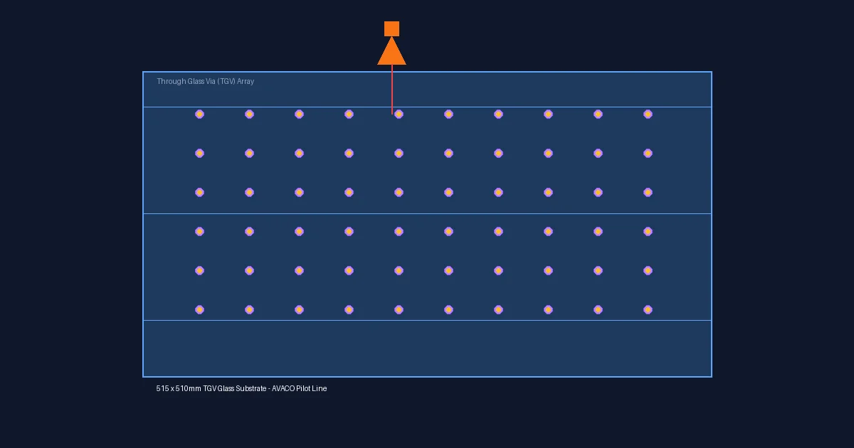
Korean advanced equipment manufacturer AVACO Co., Ltd. (KRX: 083930) announced on August 11, 2026 that it has begun operating a 515x510mm Through Glass Via (TGV) pilot production line, marking a significant milestone in the semiconductor industry’s push toward glass-based substrate technologies for next-generation advanced packaging applications.
The pilot line represents a collaborative effort between AVACO and AVATEC Co., Ltd. (KRX: 149150), combining AVACO’s TGV laser processing equipment technology with AVATEC’s glass etching and thin-film processing expertise. The operation covers the complete TGV process chain, including laser via formation, chemical etching, metal seed-layer deposition, and optical inspection — enabling full end-to-end process validation at panel-scale dimensions.
Reviewed by AtlasPCB Engineering Team
Why Glass Substrates Matter for Advanced Packaging
Glass substrates have emerged as a leading candidate to replace organic ABF (Ajinomoto Build-up Film) substrates in high-performance semiconductor packaging applications. The material advantages are substantial: glass offers dimensional stability an order of magnitude better than organic materials (thermal expansion coefficient closely matching silicon), superior flatness enabling finer redistribution layer lithography, and electrical properties (low dielectric constant, low loss tangent) that benefit high-frequency signal transmission.
These characteristics make glass substrates particularly attractive for AI accelerator and high-bandwidth memory (HBM) interposer applications, where chiplet-to-chiplet interconnect density continues to increase beyond what organic substrates can reliably support. Intel, Samsung, and several Japanese substrate manufacturers have publicly committed to glass substrate programs, creating significant demand for the specialized equipment and process capabilities that AVACO and AVATEC are now demonstrating at pilot scale.
AVACO’s TGV Technology Platform
The core of AVACO’s TGV capability is its second-generation laser processing system, the AXIUM AP-250K. This system employs dual optical heads to achieve processing speeds of approximately 10,000 vias per second while maintaining positional accuracy within ±5μm — tolerances required for the via densities demanded by advanced fan-out and interposer packaging architectures.
AVACO has invested in TGV equipment development since 2023, progressively building a comprehensive solution that extends beyond laser drilling. The company’s portfolio now includes alkaline-based glass etching equipment (for via sidewall smoothing after laser processing), seed-layer deposition systems using PVD and hybrid deposition methods, and optical inspection equipment for automated defect detection and quality control across the full process flow.
The high-aspect-ratio TGV process development is particularly significant. Unlike through-silicon vias (TSVs) in silicon interposers, TGVs in glass substrates must contend with the brittle fracture characteristics of glass and the challenge of achieving conformal metal coverage on glass via sidewalls. AVACO’s integrated approach — controlling both the via formation and subsequent metallization steps — addresses these challenges within a single validated process ecosystem.
Partnership Structure and Commercialization Timeline
The AVACO-AVATEC partnership leverages complementary strengths. AVACO contributes equipment technology and TGV process development, while AVATEC provides operational expertise derived from its experience in display glass etching and thin-film processing. This combination allows pilot-line operations to be evaluated from both a technology development and a mass-production readiness perspective.
During the first half of 2026, the partners secured glass material supply agreements through NDAs with major glass material suppliers, completing the raw material supply chain necessary for sustained pilot operations. The companies plan to provide TGV glass substrate samples ranging from 100x100mm to 515x510mm by end of 2026, covering laser-drilled and seed-layer-deposited substrates.
From 2027, the roadmap expands to include fully metallized samples with via filling and planarization — the final process steps required before glass substrates can enter package assembly integration. Both companies are actively discussing technology cooperation and mass-production equipment opportunities with multiple overseas customers, signaling that the commercialization pathway extends beyond the Korean domestic market.
Industry Context: The Glass Substrate Race Intensifies
AVACO’s pilot line announcement arrives amid intensifying global competition in glass substrate development. Intel commenced pilot production at its Rio Rancho, New Mexico facility earlier this year, targeting glass substrates for its next-generation data center processors. Samsung Electro-Mechanics has developed terahertz-frequency inspection systems specifically for glass substrate quality control. China’s glass substrate consortium (GCPA) has coordinated domestic investment in TGV research across multiple university and industry partners.
The 515x510mm panel size that AVACO has achieved is particularly notable. This dimension matches the large-format panel processing standard that the industry is converging upon for next-generation substrates, enabling higher unit count per panel and lower per-unit processing cost compared to smaller panel formats. The ability to demonstrate TGV process control across this large format — where thermal uniformity, laser positioning accuracy, and deposition thickness uniformity become significantly more challenging — represents genuine process maturity.
Implications for the PCB and Substrate Industry
The progression of glass substrates from laboratory demonstrations to pilot-line validation signals that the technology is approaching the commercial readiness required for adoption in volume semiconductor packaging. For the broader PCB and substrate manufacturing ecosystem, this development has several implications.
Traditional organic substrate manufacturers face increasing competitive pressure in the highest-performance market segment. While ABF substrates will continue to dominate mainstream packaging applications for the foreseeable future, the premium tier — occupied by AI accelerator interposers, advanced HBM packaging, and photonic integration — is migrating toward glass-based solutions that offer superior dimensional control and electrical performance.
Equipment manufacturers like AVACO are positioning themselves at the center of this transition, providing the capital equipment that both established substrate manufacturers and new market entrants will require to build glass substrate production capacity. The company’s strategy of combining equipment sales with pilot-line demonstration lowers the barrier for potential customers to evaluate and adopt TGV technology.
For PCB design engineers, the eventual commercialization of glass substrates at scale will enable new packaging architectures with tighter via pitches, finer redistribution layers, and larger interposer dimensions than currently possible with organic substrates. These advances will propagate through the design chain as package-level improvements that enable smaller, faster, and more power-efficient electronic systems.
Sources: IC&PCB Union (August 11, 2026), AVACO Co., Ltd. investor relations disclosure
About AtlasPCB — We specialize in complex PCB manufacturing for HDI, RF, and high-reliability applications. Explore our impedance-controlled PCB manufacturing . Every order includes free engineering review. Get your quote.
Reviewed by AtlasPCB Engineering Team — IPC-certified manufacturing specialists with 15+ years of production experience in HDI, RF, and high-reliability PCB fabrication. Content based on factory floor data and real customer design reviews.
- glass substrate
- TGV
- advanced packaging
- semiconductor
- AVACO
- AVATEC
- PCB industry news