· AtlasPCB Engineering · News · 7 min read
Shinko Electric Develops 22-Layer Glass Substrate While Samsung Electro-Mechanics Faces Production Delays
Shinko Electric Industries has successfully developed a 22-layer glass substrate using 11 copper wiring layers on each side of a glass core, solving the SeWaRe crack problem through polymer edge protection. Meanwhile, Samsung Electro-Mechanics' mass production timeline slips to 2028 or later, giving Japanese companies an early technology lead in the glass substrate race for AI chip packaging.

The race to commercialize glass substrates for next-generation AI chip packages took a significant turn on August 15, 2026, when industry sources reported that Shinko Electric Industries (TYO: 6967) had successfully developed a 22-layer glass substrate. The Japanese semiconductor package substrate maker achieved this milestone by stacking eleven copper wiring layers on each side of a glass core, demonstrating the high-density interconnect capability that AI accelerator packages will demand as die sizes and I/O counts continue to grow beyond what organic substrates can reliably support.
Shinko Electric’s achievement is notable not just for the layer count but for how the company solved one of the fundamental reliability challenges in glass substrate manufacturing: the SeWaRe problem. SeWaRe refers to stress-induced cracks or delamination that form inside the glass during processing or thermal cycling, particularly at substrate edges where stress concentrates during the repeated thermal excursions of multilayer buildup processing and subsequent assembly reflow. The company addressed this by applying a proprietary polymer-based protective material to the glass substrate edges, which disperses the concentrated stress during thermal loading and prevents SeWaRe defects even after repeated heat exposure cycles. This edge-protection approach represents a practical engineering solution to what has been one of the industry’s most persistent glass substrate reliability barriers.
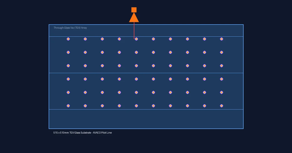
Beyond the SeWaRe solution, Shinko Electric has also developed through-glass via (TGV) technology for forming microscopic vertical holes through the glass core, along with processes for building multiple insulation and copper wiring layers. Together, these capabilities enable the 22-layer structure with the wiring density required for advanced AI packages that integrate multiple processor dies and high-bandwidth memory stacks. The company showcased its latest glass-core substrate at the Advanced Packaging Summit 2026 in July, demonstrating both the technical viability and the manufacturing readiness of its approach.
Why Glass Substrates Matter for AI Hardware
The fundamental driver behind the glass substrate race is the physical limitation of conventional organic substrates. Current ABF (Ajinomoto Build-up Film) substrates exhibit measurable warpage when package sizes exceed approximately 70mm per side, which creates assembly yield problems during flip-chip bonding and underfill dispensing. As AI accelerators push toward 100mm or larger package dimensions to accommodate bigger die sizes and expanded chiplet configurations, this warpage problem becomes a hard barrier that no amount of process optimization on organic materials can overcome.
Glass substrates offer three intrinsic advantages that make them the leading candidate for next-generation packaging. First, glass has a coefficient of thermal expansion (CTE) of approximately 3.2 ppm per degree Celsius, closely matching silicon’s 2.6 ppm — far better than organic substrates at 12-16 ppm. This CTE match dramatically reduces thermomechanical stress at the die-to-substrate interface during thermal cycling. Second, glass is dimensionally stable under thermal load, meaning it does not warp or bow the way organic materials do at large panel sizes. Third, glass supports much finer TGV pitch (down to 100um or below) compared to through-hole vias in organic substrates, enabling higher I/O density in the same footprint.
For the PCB and electronics manufacturing ecosystem, the transition to glass substrates represents a fundamental technology shift in how advanced packages connect to the outside world. While glass substrates will initially target only the highest-performance AI and HPC packages, the manufacturing techniques being developed — including TGV formation, multilayer wiring, and advanced plating — will eventually influence mainstream substrate and high-density interconnect PCB technology.
Japanese Companies Take the Early Lead
Shinko Electric’s 22-layer demonstration positions Japanese companies at the forefront of glass substrate commercialization. The broader Japanese effort includes multiple participants at various stages of readiness.
Dai Nippon Printing (DNP) established a TGV glass substrate pilot line in Saitama in December 2025 and began supplying samples to customers in 2026, with mass production targeted for 2028. AGC (formerly Asahi Glass) has been supplying glass core substrates to multiple development partners, leveraging its expertise in specialty glass manufacturing. Together with Shinko Electric, these companies form a Japanese ecosystem that spans glass material supply, via formation, and multilayer substrate buildup.
The Japanese lead is significant because it emerged from existing competencies in precision glass manufacturing, thin-film deposition, and advanced package substrate production that were already world-class before the glass substrate race began. Shinko Electric, as a subsidiary of Fujitsu, has decades of experience in flip-chip BGA package substrates and IC carrier manufacturing, providing the foundation for extending its capabilities to glass cores.
Samsung Electro-Mechanics Faces Delays
In contrast to the Japanese progress, Samsung Electro-Mechanics (KRX: 009150) is experiencing timeline pressures in its glass substrate program. The company has been pursuing commercialization through GlaSSEM, a joint venture with Dongwoo Fine-Chem focused specifically on glass substrate manufacturing. While Samsung Electro-Mechanics is conducting customer validation and sample evaluations for large-area, high-layer-count glass substrates targeting data center applications, its equipment-order and production-line schedules remain uncertain following multiple delays.
Industry sources suggest that additional prototype qualification rounds may push Samsung Electro-Mechanics’ mass production timeline to 2028 or later, potentially allowing Japanese and other competitors to establish production capability and customer relationships first. The delays appear related to both equipment procurement challenges and the need for additional development cycles to achieve the yield levels required for production economics.
This situation mirrors the broader competition in advanced semiconductor packaging: while Korean companies have scale advantages in conventional substrate manufacturing, the transition to fundamentally new materials like glass requires building new process knowledge that does not directly transfer from existing organic substrate lines. The SeWaRe problem that Shinko solved with polymer edge protection is one example of a glass-specific challenge that each company must independently address.
Advanced Substrate-Like PCB Capabilities
While glass substrates remain in development, AtlasPCB manufactures HDI boards with substrate-like features: stacked microvias, 75um trace and space, any-layer interconnects, and ultra-thin constructions down to 0.2mm. For current-generation AI and networking hardware, our advanced HDI capabilities bridge the gap until glass substrates reach production.
Request an Advanced HDI QuoteWhat This Means for PCB Engineers Today
The glass substrate timeline — with mass production now realistically targeted for 2028-2029 — means that for the next two to three years, advanced interconnect designs will continue to rely on organic substrates and high-density PCB technology for all but the most extreme AI accelerator packages. Engineers designing current-generation hardware should plan their interconnect strategy around the capabilities available today: HDI PCB with sequential lamination, advanced buildup structures up to 5+N+5, and via-in-pad with copper-filled microvias.
However, the glass substrate developments signal where the industry is heading. Design methodologies that assume organic substrate behavior — including warpage compensation in assembly tooling, CTE-mismatch-aware BGA pad design, and thermal cycling derating for package-level interconnects — will need revision as glass substrates enter production. Engineers working on products with 3-5 year development cycles for defense, aerospace, or automotive applications should begin tracking glass substrate qualification data from their substrate suppliers.
The competitive dynamics between Japanese companies (Shinko, DNP, AGC) and Korean companies (Samsung Electro-Mechanics via GlaSSEM) will determine pricing and availability once production begins. For PCB designers and system architects, the key watchpoint is whether glass substrates reach cost parity with advanced organic substrates at volume — a threshold that depends on yield improvements that remain to be demonstrated at production scale.
Sources: IC&PCB Union (ic-pcb.com), industry reports from Advanced Packaging Summit 2026.
Related Reading:
About AtlasPCB — We specialize in complex PCB manufacturing for HDI, RF, and high-reliability applications. Explore our impedance-controlled PCB manufacturing . Every order includes free engineering review. Get your quote.
Reviewed by AtlasPCB Engineering Team — IPC-certified manufacturing specialists with 15+ years of production experience in HDI, RF, and high-reliability PCB fabrication. Content based on factory floor data and real customer design reviews.
- glass substrate
- advanced packaging
- Shinko Electric
- Samsung Electro-Mechanics
- AI chips
- TGV
- semiconductor packaging
- interposer