· AtlasPCB Engineering · Engineering · 12 min read
PCB DFM Check for Rigid-Flex: Bend Zone Design Rules That Prevent Field Failures
A manufacturing-focused DFM guide for rigid-flex PCB bend zones — covering minimum bend radius calculations, copper routing rules, coverlay specifications, stiffener placement, and the design violations we catch most frequently during pre-production review.
Quick Answer
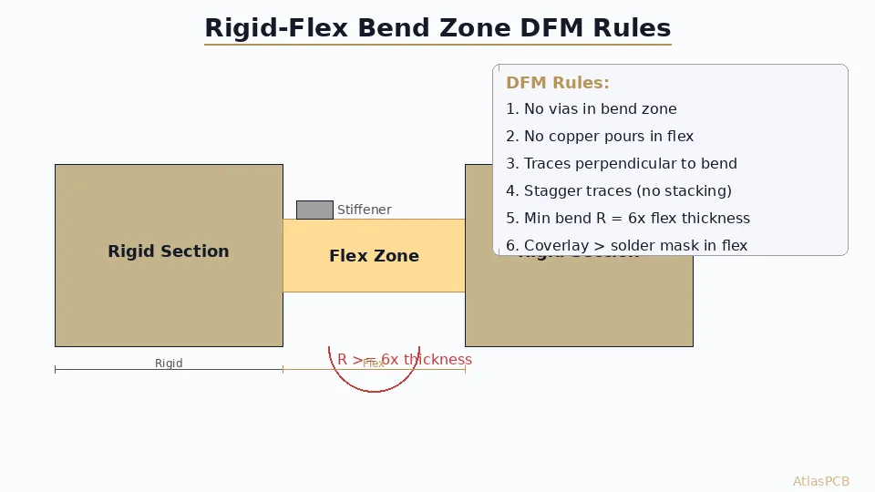
The critical DFM rules for rigid-flex bend zones are: minimum bend radius must equal 6x the flex thickness for dynamic applications (10x for >100K cycles), traces must route perpendicular to the bend axis with staggered (not stacked) placement on multi-layer flex, no vias or plated features within the bend zone, coverlay replaces solder mask in flex areas, and stiffeners must extend at least 1.5mm past the rigid-to-flex transition to prevent stress concentration at the junction.
Quick Answer: The 8 DFM Rules for Rigid-Flex Bend Zones
| Rule | Requirement | Why It Matters |
|---|---|---|
| 1. Bend radius | Min 6x flex thickness (dynamic) | Copper fatigue life |
| 2. Trace direction | Perpendicular to bend axis | Prevent tensile cracking |
| 3. Trace stacking | Staggered across layers (not aligned) | Neutral axis optimization |
| 4. No vias in bend | Zero plated features in flex zone | Via barrels crack under flex |
| 5. No copper pour | Hatched pattern or traces only | Solid copper resists bending |
| 6. Coverlay, not mask | Polyimide coverlay in all flex areas | Solder mask is brittle |
| 7. Stiffener overlap | Min 1.5mm past rigid-flex junction | Prevent stress concentration |
| 8. Adhesive control | No excess adhesive squeeze-out | Stiff spots cause localized stress |
If your rigid-flex design passes all eight rules, it will survive its intended flex life. If it violates even one, the failure mode is typically catastrophic — a cracked trace in a bend zone means a dead product.
The Physics of Bend Zone Failure
Understanding why these DFM rules exist requires a basic appreciation of how bending loads distribute through a flexible PCB cross-section. When a flex circuit bends around a radius R, the outer surface experiences tensile strain and the inner surface experiences compressive strain. At the geometric center — the neutral axis — strain is zero.
For a single-layer flex construction (one copper layer, one polyimide film, one coverlay), the neutral axis sits roughly at the center of the total thickness. Copper on the outer radius stretches; copper on the inner radius compresses. Electrodeposited copper (ED copper) tolerates approximately 10-15% elongation before cracking, while rolled-annealed copper (RA copper) handles 20-30%. This is why RA copper is specified for dynamic flex applications — it has roughly twice the fatigue life at equivalent strain levels.
The minimum bend radius formula ensures that copper strain stays below the fatigue limit. For a flex section total thickness t and bend radius R, the outer surface strain is approximately t/(2R). Setting strain below 1.5% for dynamic applications gives the 6x ratio: R/t = 1/(2 x 0.015) ≈ 33 — but IPC-2223 uses empirical safety factors accounting for manufacturing variation, reducing this to the 6x guideline for single-layer. Multi-layer constructions have their neutral axis shifted (or multiple neutral axes between layers), which is why the ratio increases to 12x and 24x for 2-layer and 3+ layer flex respectively.
In our production, we see this physics play out when customers try to “cheat” the bend radius on multi-layer flex designs. A 4-layer flex section (total flex thickness approximately 0.25mm) with a specified 2mm bend radius (8x, within guideline) works perfectly for static flex. But the same design subjected to 10,000 flex cycles during product life — say, a folding phone hinge or a robotic arm joint — will develop micro-cracks in the outer copper layer between cycles 5,000-8,000. The fatigue data is unambiguous.
RIGID-FLEX DFM REVIEW
Catch Bend Zone Errors Before Fabrication
Our process engineers review every rigid-flex design for bend radius, trace routing, coverlay specification, and transition geometry. Issues found: zero cost. Issues missed: board respin.
Submit Design for Review ›
Rule 1: Minimum Bend Radius Calculation
The industry-standard minimum bend radius varies by construction type, copper type, and application:
| Flex Construction | Dynamic Flex (>10K cycles) | Static Flex (install once) |
|---|---|---|
| 1-layer, RA copper | 6x thickness | 3x thickness |
| 1-layer, ED copper | 12x thickness | 6x thickness |
| 2-layer, RA copper | 12x thickness | 6x thickness |
| 2-layer, ED copper | 24x thickness | 12x thickness |
| 3+ layer | Case-by-case (24x+ minimum) | 12x minimum |
Practical example: A 2-layer flex section with 0.5oz RA copper, 25um polyimide base, 25um coverlay top and bottom has a total flex thickness of approximately 0.14mm. For dynamic flex, minimum bend radius = 12 x 0.14mm = 1.68mm. Rounding up to 2mm provides manufacturing margin.
The DFM check we perform: We measure your specified bend radius from Gerber data (or mechanical drawings if provided) and compare against the calculated minimum for your actual flex stackup thickness. If your design calls for a tighter radius than the construction supports, we flag it and propose either a thinner flex section (remove a copper layer, reduce polyimide thickness) or a larger housing radius.
Rule 2: Trace Routing Direction
This rule is non-negotiable and represents the single most common DFM violation we encounter — appearing in approximately 35% of new rigid-flex designs submitted to us. Traces in the flex zone must run perpendicular to the bend axis.
When a trace runs parallel to the bend, it experiences the full bending strain along its entire length within the flex zone. A 50mm-long parallel trace in a bend zone has 50mm of copper simultaneously under tensile stress. Even with RA copper, this trace will develop a fatigue crack at some point along its length — and you cannot predict where.
When a trace runs perpendicular to the bend, only a tiny cross-section of the trace (the width of the trace, typically 0.1-0.3mm) is under bending strain at any given point. The strain distributes across the conductor width rather than accumulating along its length. This geometric advantage makes perpendicular routing orders of magnitude more fatigue-resistant.
What if I must route a signal parallel to the bend? You have two options. First, redesign the connector placement so the signal enters the flex section perpendicular to the bend axis. Second, if routing direction is constrained, use curved trace paths (S-curves) that continuously change the stress distribution point along the trace, and significantly increase the bend radius beyond minimum.
Rule 3: Stagger Traces Across Layers
On multi-layer flex sections (2 or more copper layers in the flex zone), traces on different layers must not be vertically aligned. When traces stack directly above each other, they create a localized thickening of the cross-section — a “beam” effect that shifts the neutral axis and concentrates bending strain at the edges of the stacked region.
The correct approach is to offset traces on adjacent layers by at least one trace width. This distributes the copper mass evenly across the flex cross-section, maintaining a predictable neutral axis position and equalizing strain distribution.
In practice, achieving perfect staggering is sometimes difficult due to routing constraints. When you cannot avoid some trace alignment, ensure those overlapping sections do not coincide with the point of maximum curvature (the apex of the bend). Place any unavoidable overlap in the straight transition region between the rigid section and the bend apex, where strain is lower.
RIGID-FLEX MANUFACTURING
22 Layers, 6 Flex Zones — We Build It
Complex rigid-flex with multiple bend zones, controlled impedance, and blind/buried vias. Up to 22-layer rigid-flex with our sequential lamination process.
View Rigid-Flex Capabilities ›Rules 4-6: Vias, Copper Pour, and Coverlay
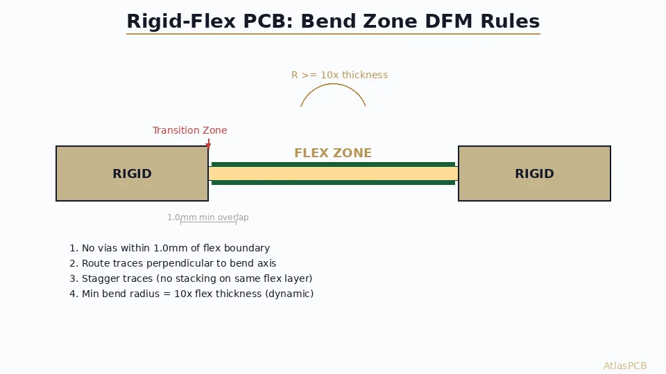
No vias in bend zones — plated through-holes and microvias have rigid copper barrel walls that do not flex. Under bending, the via barrel cracks, the internal copper connection fractures, and you get an intermittent open circuit that is nearly impossible to diagnose in the field. Our DFM check flags any via whose center falls within the defined flex zone boundary (including the 1mm transition buffer zone on each side).
No solid copper pour in flex — a solid copper plane in a flex zone acts like a sheet metal spring. It resists bending, creates massive stress concentration at its edges, and will crack at the boundary between pour and no-pour. If you need a ground reference in the flex zone, use a cross-hatch pattern with 50% or less copper coverage. The hatch lines must also be perpendicular to the bend axis. Better still, eliminate ground planes entirely from the flex zone and use ground traces alongside signal traces (coplanar waveguide structure if impedance control is needed in the flex section).
Coverlay specification — this is a material substitution issue that should be caught at the stackup design stage, not during DFM review. Yet we still see designs where the engineer specifies LPI solder mask on flex layers, likely because their EDA tool defaults to solder mask everywhere. Solder mask is an epoxy-based material that cracks after even a single 90-degree bend. Coverlay (polyimide film bonded with acrylic adhesive) flexes indefinitely without damage. The material substitution is straightforward but must be specified in the fabrication drawing.
Rule 7: Stiffener Design at Rigid-Flex Transitions
The rigid-to-flex transition is the highest-stress region in any rigid-flex assembly. At this boundary, the PCB goes from fully rigid (infinite effective bend radius) to flexible within a few millimeters. Without proper transition engineering, 100% of the bending strain concentrates at this single line — like folding a piece of paper at a hard crease instead of a gentle curve.
Stiffeners serve two purposes at transitions: they extend the rigid zone slightly into the flex area (preventing the abrupt stiffness change) and they create a graduated stiffness profile where the effective rigidity tapers off over 1.5-3mm rather than dropping instantaneously.
Design rules for stiffener overlap:
- Minimum overlap into flex zone: 1.5mm from the rigid-flex boundary
- Stiffener material: typically FR-4 or polyimide sheet, 0.1-0.3mm thick
- Adhesive: pressure-sensitive or thermosetting (must not stiffen the flex zone beyond the intended support region)
- Taper: if possible, taper the stiffener thickness from full at the rigid boundary to zero at its flex-zone edge
Our process engineers evaluate stiffener geometry during DFM review and have specific recommendations based on the flex thickness, bend radius, and expected cycle life. We have seen too many designs where the mechanical engineer assumed the rigid-flex junction was inherently strong — it is not, and stiffener design is what makes it reliable.
ENGINEERING CONSULTATION
First-Time Rigid-Flex Design?
Our applications engineers can review your mechanical constraints and recommend stackup, bend radius, stiffener placement, and material selection before you finalize your layout.
Get Recommendation ›Real-World DFM Catches From Our Production
To illustrate why pre-production DFM review matters specifically for rigid-flex, here are anonymized examples from designs we reviewed in the past quarter:
Case 1: Wearable health monitor — 4-layer rigid-flex, 2 flex zones connecting sensor board to main processor board. The designer routed a high-speed SPI bus (4 traces) parallel to the bend axis across both flex zones. Our DFM review caught this; the designer re-routed with connector placement changes that allowed perpendicular routing. Without this catch, the SPI traces would have failed within the product’s 2-year warranty period at the expected 5,000+ bend cycles.
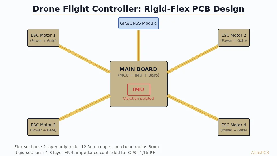
Case 2: Drone flight controller — 6-layer rigid-flex with 3 flex zones. The design included ground pour on both flex layers to maintain impedance control through the flex section. We recommended a cross-hatch ground pattern (45-degree hatch, 0.2mm line, 0.4mm pitch) which maintained >90% of the impedance control performance while eliminating the solid copper failure mode.
Case 3: Industrial robot joint — 8-layer rigid-flex specified for 200,000+ dynamic flex cycles. The original design had a 3mm bend radius on a 0.22mm flex section (13.6x ratio — technically within the 12x minimum for 2-layer). We recommended increasing to 4mm (18x) based on our fatigue test data showing that margins above minimum significantly improve high-cycle reliability. The customer accepted, modified their housing, and achieved the 200K cycle target in qualification testing.
Submitting a Rigid-Flex Design for DFM Review
When you send a rigid-flex design for manufacturing quotation and DFM review, include these documents for the fastest and most thorough review:
- Gerber files — complete fabrication set including all layers, drill files, and layer stack definition
- Mechanical drawing (PDF or DXF) — showing flex zone boundaries, intended bend radii, and fold directions
- Fab drawing — specifying materials per layer (rigid vs. flex), coverlay openings, and stiffener locations
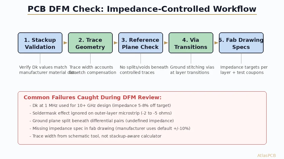
- Impedance requirements — if any controlled-impedance traces pass through or near flex zones
- Application description — static vs. dynamic flex, expected bend cycle count, operating temperature range
The more context we have about your mechanical application, the better our DFM recommendations. A flex zone designed for “install once and forget” (a folded board inside a laptop) has fundamentally different DFM requirements than one designed for “bend 100,000 times” (a foldable phone hinge or robotic cable replacement).
ATLASPCB
Upload Your Rigid-Flex Design for DFM Review
Bend zone analysis, stiffener recommendations, and material specification review — all before you commit to production. Up to 22-layer rigid-flex with multiple flex zones.
Upload Design ›
Reviewed by AtlasPCB Engineering Team — 15+ years in advanced PCB fabrication for RF, HDI, and rigid-flex applications.
Related Reading:
About AtlasPCB — We specialize in complex PCB manufacturing for HDI, RF, and high-reliability applications. Explore our rigid-flex PCB manufacturing, free engineering DFM review, or get an full PCB manufacturing capabilities . Every order includes free engineering review. Get your quote.
Reviewed by AtlasPCB Engineering Team — IPC-certified manufacturing specialists with 15+ years of production experience in HDI, RF, and high-reliability PCB fabrication. Content based on factory floor data and real customer design reviews.
Frequently Asked Questions
What is the minimum bend radius for rigid-flex PCB?
Can I route traces parallel to the bend axis in rigid-flex?
Why do rigid-flex PCBs fail at the rigid-to-flex transition?
Should I use solder mask or coverlay in the flex section?
What DFM errors do you catch most frequently on rigid-flex designs?
- PCB DFM check
- rigid-flex PCB manufacturer
- rigid-flex PCB design
- PCB manufacturing
- DFM verification