· AtlasPCB Engineering · Engineering · 10 min read
Multilayer PCB Cost in 2026: Complete Pricing Model from 4 Layers to 20+ Layers
Transparent breakdown of multilayer PCB pricing in 2026 covering how layer count, material choice, hole technology, and volume affect unit cost. Includes real pricing data for 4, 6, 8, 10, 12, 16, and 20-layer boards with specific cost drivers at each tier and optimization strategies to keep your BOM under control.
Quick Answer
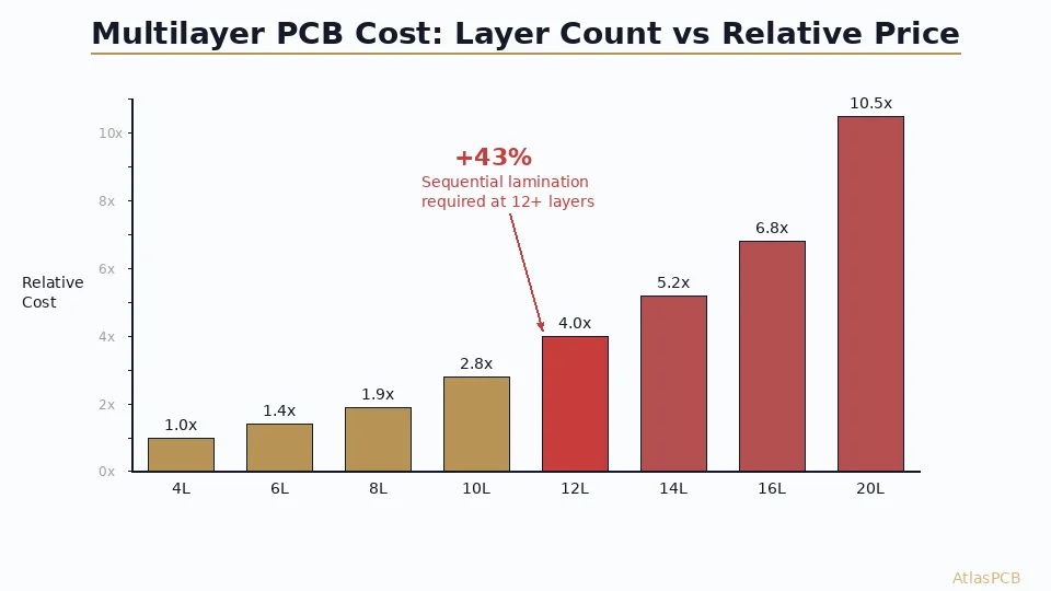
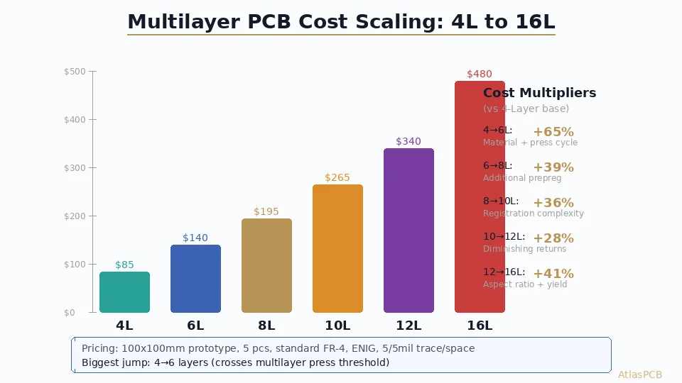
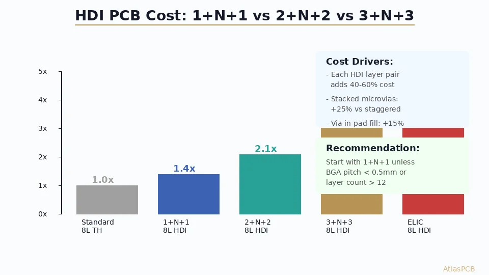
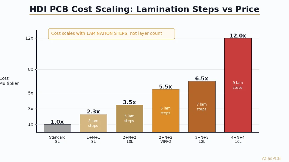
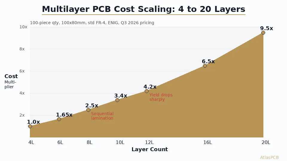
Multilayer PCB cost does not scale linearly with layer count. A 6-layer board costs roughly 1.5-1.8x a 4-layer. The first major jump occurs at 8 layers (2.2-2.8x) due to sequential lamination. The second jump hits at 12+ layers (3.5-5x) where material waste, registration tolerances, and yield loss compound. HDI construction (microvias) adds 30-60% premium over through-hole-only designs of equivalent layer count. In 2026, copper and laminate material costs have risen 15-25% from 2024 levels due to AI server demand absorbing high-end CCL capacity.
Quick Reference: 2026 Multilayer PCB Pricing Ranges
Pricing below is for standard FR-4, 1oz copper, ENIG finish, 100-piece quantity, 100x80mm board size, mechanical drill only (no HDI). Prices reflect Q3 2026 market conditions.
| Layer Count | Price Range (per board) | vs 4-Layer Multiplier | Key Cost Driver |
|---|---|---|---|
| 4-layer | $6-12 | 1.0x (baseline) | Standard single lamination |
| 6-layer | $10-18 | 1.5-1.8x | Additional lamination + imaging |
| 8-layer | $18-32 | 2.2-2.8x | Thinner cores, tighter registration |
| 10-layer | $28-48 | 3.0-3.8x | Sequential lamination typical |
| 12-layer | $40-70 | 3.5-5.0x | Yield drops, material waste up |
| 16-layer | $65-110 | 5.5-8.0x | Registration critical, yield-sensitive |
| 20-layer | $95-160 | 7-12x | Premium materials, low yield tolerance |
Note: These are bare board costs only. Assembly, components, and testing are separate. Pricing varies +/-30% based on specific requirements (impedance control, heavy copper, tight tolerances).
Understanding the Cost Curve: Why It Is Not Linear
Engineers often assume that doubling layer count roughly doubles cost. The reality is more nuanced — and understanding the actual cost structure helps you make informed design decisions about layer count versus alternative routing strategies.
PCB manufacturing cost has five main components, and their relative contribution shifts dramatically with layer count:
Material cost (30-50% of total): Copper-clad laminate is priced per square foot per layer. But thinner cores required for high layer counts cost more per unit area than thick cores. A 3mil core (common in 16+ layer boards) costs roughly 2.5x per square foot compared to 12mil core (standard in 4-layer boards). Material cost scales slightly worse than linear with layer count.
Processing cost (25-35% of total): Each layer requires imaging, developing, etching, and inspection. But processing cost per layer decreases slightly at higher layer counts because setup is amortized. The exception is lamination — each sequential press cycle adds significant cost and is the primary driver of the price jumps at 8 and 12 layers.
Drilling cost (10-20% of total): Through-hole drilling cost is roughly constant regardless of layer count (same number of holes, slightly longer drill travel). But high layer counts often require controlled-depth drilling (blind/buried vias) or laser drilling (microvias), which add 25-60% to drilling cost.
Yield loss (10-25% at high layer counts): This is the hidden cost multiplier. A 4-layer board might achieve 95% first-pass yield. A 12-layer board with tight trace/space achieves 80-85%. A 20-layer board may run at 70-75% yield. Every scrapped panel is fully processed material thrown away — the manufacturer must build extra panels to deliver your quantity, and that overage is priced into your unit cost.
Testing cost (5-10%): Electrical testing time increases with layer count due to more nets to verify. Flying probe testing a 20-layer board takes 3-5x longer than a 4-layer board of similar size.
TRANSPARENT PRICING
Instant Multilayer PCB Quote — No Hidden Fees
Upload your Gerber files for an instant quote with full cost breakdown by layer count, material, and finish. See exactly what drives your unit price.
Get Instant Quote ›
The Three Price Breakpoints Every Engineer Should Know
Breakpoint 1: 4-Layer to 6-Layer (Moderate Jump, 1.5-1.8x)
Moving from 4 to 6 layers adds one lamination cycle (now bonding two cores with one prepreg layer instead of one core with two prepreg layers), one additional inner-layer imaging step, and slightly tighter registration requirements. The cost increase is modest because the same equipment and process flow handles both — no fundamentally new capability is required.
When 6 layers make financial sense: If your 4-layer design requires 4/4mil trace/space to achieve routing (versus comfortable 5/5mil on 6 layers), the yield improvement on 6 layers at relaxed rules often costs less than the tighter-tolerance surcharge on a dense 4-layer. We see this crossover frequently on BGA designs where escape routing drives density.
Breakpoint 2: 6-Layer to 8-10 Layer (Significant Jump, 2.2-3.8x)
The jump to 8+ layers introduces several simultaneous cost increases. Cores thin to 4-8mil (more expensive, more fragile to handle), registration tolerances tighten to +/-2mil (versus +/-3mil for 4-6 layer), and many 8-layer designs require buried vias that necessitate sequential lamination (multiple press cycles — each cycle adds 20-30% to processing cost).
At 10 layers, nearly all designs require sequential lamination regardless of via structure, simply because achieving uniform dielectric thickness across 10 layers demands controlled pressing in stages rather than a single “bookbuild” press. The material waste also increases: inner layers that fail inspection before lamination represent lost material across all layers bonded to them.
Breakpoint 3: 12-Layer to 16+ Layer (Steep Jump, 5-12x)
Above 12 layers, several factors compound aggressively. Material costs are amplified by the “sandwich effect” — a single inner-layer defect detected after lamination scraps the entire panel including all good layers bonded to it. Manufacturers build 15-25% overage into production quantities to ensure delivery, and that overage cost is embedded in your unit price.
Registration across 16+ layers requires specialized equipment (laser direct imaging with optical registration systems reading fiducials on every layer). Many shops cannot achieve the +/-1.5mil layer-to-layer registration required for 16-layer designs with 4/4mil trace/space — limiting your vendor pool to better-equipped (and more expensive) facilities.
Additionally, at 16+ layers, standard FR-4 dielectric thickness between layers may not meet impedance targets without using exotic thin prepregs (2-3mil), which are both expensive and hard to source in 2026 due to AI server demand consuming premium thin-dielectric materials.
2026 Market Conditions Affecting Multilayer Pricing
The PCB material market in 2026 is significantly different from 2023-2024, primarily due to AI server manufacturing consuming high-end materials at unprecedented volumes:
Copper foil: Prices up 18-22% from 2024. Electrodeposited copper foil for inner layers is in tight supply as AI server boards (24-30 layers with 2oz copper on power planes) consume massive quantities. RTF and VLP copper foil (required for high-speed signal layers) commands 40-60% premiums over standard ED copper.
High-performance CCL: Megtron 6, TU-872, and similar low-loss laminates have 12-16 week lead times versus 4-6 weeks in 2024. These materials are being allocated primarily to AI server and networking switch manufacturers. Designs using standard FR-4 are largely unaffected, but any board requiring low-loss dielectric (10+ Gbps signals, RF applications) faces longer lead times and 15-30% price increases.
Thin cores: 3-4mil cores (essential for 16+ layer boards maintaining reasonable total thickness) are scarce. Many manufacturers have shifted production capacity toward 6-8mil cores optimized for AI server stackups. If your design requires 3mil cores, discuss availability with your manufacturer early — substituting 4mil cores might require stackup redesign but avoids 6-8 week material delays.
Practical impact for most designs: Standard 4-8 layer boards on conventional FR-4 have seen moderate cost increases (8-12%) that are manageable. The severe supply tightness primarily affects 12+ layer boards with controlled impedance and specialty materials. If your design can use standard FR-4 with 6mil or thicker cores, pricing remains relatively accessible.
MULTILAYER PCB EXPERTISE
4 to 30 Layers — Standard and HDI Construction
We manufacture boards from simple 4-layer to complex 30-layer HDI with stacked microvias. Material in stock for most standard stackups.
View HDI Capabilities ›Cost Optimization Strategies: Reducing Layer Count Without Compromising Design
The most effective cost optimization is often eliminating layers rather than negotiating price. Each layer removed saves material, processing, and yield costs simultaneously. Based on designs we have helped customers optimize:
Strategy 1: HDI microvias to replace routing layers. A 0.5mm-pitch BGA that requires 4 conventional routing layers for escape can break out in 2 HDI layers with 0.1mm microvias. The HDI premium (30-50%) on a 6-layer board is usually less than the cost of an 8-layer conventional board. This approach works particularly well for designs where BGA escape is the sole driver of layer count — if your actual signal routing fits in fewer layers once BGAs are escaped, HDI reduces total layer count and often total cost.
Strategy 2: Tighter trace/space to reduce routing layers. Moving from 5/5mil to 4/4mil trace/space increases routing density by approximately 56% (both in-trace density and between-trace packing). This may allow eliminating one or two routing layers entirely. The tighter geometry adds 10-15% to imaging and etching costs but saves an entire layer’s worth of material and processing. Cost-effective when it eliminates at least one layer.
Strategy 3: Stackup optimization for impedance. Many 8-layer designs use layers 3 and 6 purely as impedance reference planes. By choosing appropriate dielectric thicknesses and copper weights, it is sometimes possible to achieve target impedances with a 6-layer stackup using the same ground/power planes as both reference and distribution. Our stackup engineers review this possibility for every design and recommend consolidation when feasible.
Strategy 4: Blind vias for power distribution. Instead of dedicating entire layers to power planes, use blind via connections from surface components to buried power/ground planes. This can consolidate multiple power domains onto fewer planes without compromising PDN impedance, potentially eliminating 1-2 layers in power-hungry designs.
Volume Pricing: How Quantity Affects Multilayer Cost
Volume pricing for multilayer PCBs follows a predictable curve with two distinct phases:
Phase 1 (1-100 pieces): NRE-dominated pricing. Tooling, programming, and setup costs are amortized over few boards. A 10-layer board that costs $50/unit at 10 pieces might cost $35/unit at 50 pieces — the per-unit NRE drop is steep. At this phase, negotiating NRE waiver or pooling with other orders provides the best savings.
Phase 2 (100-10,000 pieces): Material-dominated pricing. Above 100 pieces, NRE is negligible per unit and material + processing dominate. Price reductions come from panel fill optimization (more boards per production panel), bulk material purchasing, and optimized production scheduling. Typical volume discount: 15-25% from 100 to 1,000 pieces, additional 10-15% from 1,000 to 5,000.
Phase 3 (10,000+ pieces): Yield and capacity negotiation. At high volumes, yield improvement becomes the primary cost lever. Manufacturers invest in process optimization for repeat orders — fine-tuning etch parameters, press profiles, and test fixtures for your specific design. Mature high-volume boards achieve 3-5% higher yield than first-run production, and that improvement flows to pricing.
For multilayer boards specifically, the volume breakpoint where per-unit cost stabilizes (where adding more quantity provides diminishing returns) is typically higher than for 2-4 layer boards — around 2,000-5,000 pieces for 8-12 layer boards versus 500-1,000 for 4-layer boards. This is because multilayer setup costs (layer registration tooling, stackup verification panels, impedance coupon design) are higher and take more volume to amortize fully.
ATLASPCB
Get Your Multilayer PCB Quote in 24 Hours
Upload Gerber files for instant pricing with full layer-by-layer cost breakdown. We show exactly what drives your board cost and recommend optimization opportunities.
Upload Gerbers and Get Quote ›
Reviewed by AtlasPCB Engineering Team — 15+ years in advanced PCB fabrication for RF, HDI, and rigid-flex applications.
Related Reading:
About AtlasPCB — We specialize in complex PCB manufacturing for HDI, RF, and high-reliability applications. Explore our HDI PCB manufacturing capabilities, multilayer PCB fabrication up to 30 layers, or get an instant online PCB quote . Every order includes free engineering review. Get your quote.
Reviewed by AtlasPCB Engineering Team — IPC-certified manufacturing specialists with 15+ years of production experience in HDI, RF, and high-reliability PCB fabrication. Content based on factory floor data and real customer design reviews.
Frequently Asked Questions
How much does a 6-layer PCB cost compared to 4-layer?
Why is there a big price jump at 8 layers?
What is the cheapest way to get more routing density without adding layers?
How much do Rogers or high-frequency materials add to multilayer PCB cost?
Has multilayer PCB pricing increased in 2026?
- multilayer PCB cost
- PCB pricing
- HDI PCB manufacturer
- PCB stackup design guide
- PCB manufacturing cost