· AtlasPCB Engineering · Engineering · 9 min read
Multilayer PCB Cost: Why 10-to-12 Layers Costs 40% More and How to Optimize
Detailed cost analysis of multilayer PCB pricing from 4 to 20 layers, explaining the sequential lamination price jump at 12 layers and proven design strategies to reduce layer count without sacrificing signal integrity or power delivery.
Quick Answer
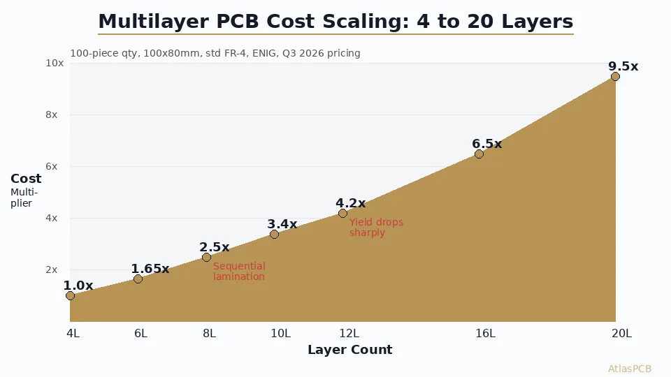
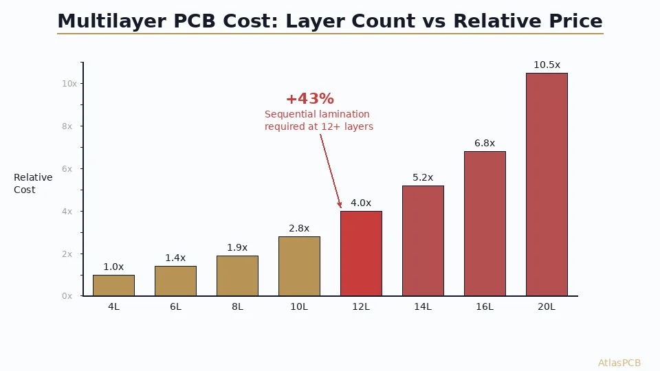
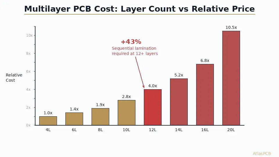
Multilayer PCB cost increases roughly 40-45% when moving from 10 to 12 layers because 12+ layer boards typically require sequential lamination (multiple press cycles) rather than single-lamination. You can often avoid this jump by using HDI microvias to route escape on fewer layers, or by optimizing your stackup to fit within 10 layers through careful power plane consolidation.
Quick Answer: Multilayer PCB Cost by Layer Count
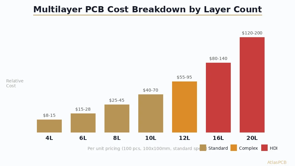
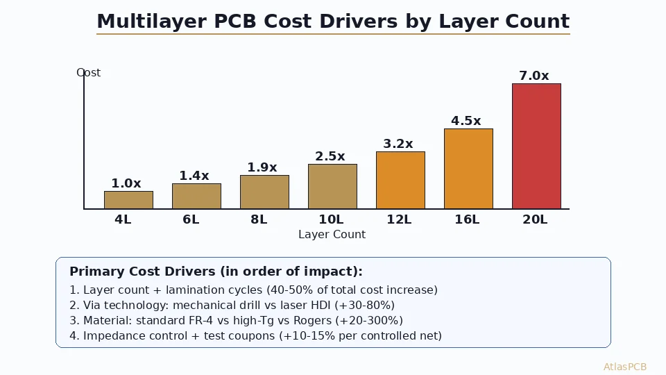
| Layers | Relative Cost | Typical Price (100x150mm, qty 100) | Key Cost Driver |
|---|---|---|---|
| 4L | 1.0x (baseline) | $12-18/pc | Single lamination, standard process |
| 6L | 1.4x | $17-25/pc | Additional prepreg + copper layers |
| 8L | 1.9x | $23-35/pc | Tighter drill aspect ratio |
| 10L | 2.8x | $45-65/pc | Maximum single-lamination complexity |
| 12L | 4.0x | $65-95/pc | Sequential lamination required |
| 14L | 5.2x | $80-120/pc | 2-stage sequential + backdrilling |
| 16L | 6.8x | $95-150/pc | Tight registration, buried vias |
| 20L | 10.5x | $140-220/pc | Multi-stage sequential, exotic drills |
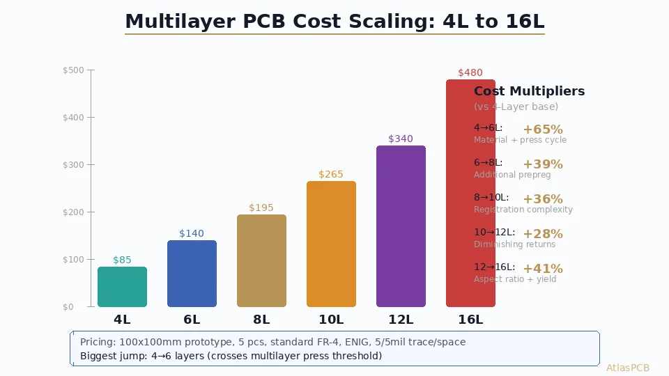
The critical insight: The 10-to-12 layer transition represents the largest single cost jump in multilayer PCB manufacturing. If you can optimize your design to fit within 10 layers, you avoid sequential lamination entirely and save 40%+ on board cost.
Why the 10-to-12 Layer Jump Exists
The cost discontinuity at 12 layers is not arbitrary — it reflects a fundamental manufacturing process boundary. Understanding why it exists helps you make informed decisions about whether to absorb the cost or redesign for fewer layers.
In a standard single-lamination process, all copper layers and prepreg sheets are stacked together and pressed in one operation. The hydraulic press applies 200-400 PSI at 180-200C for 60-90 minutes, bonding all layers simultaneously. For up to 10 layers, this process works reliably because the total stackup thickness (typically 1.6-2.4mm) allows through-hole drilling with acceptable aspect ratios (maximum 8:1 to 10:1) and the layer-to-layer registration stays within +/-3 mil across the panel.
At 12 layers and above, two physical constraints force the switch to sequential lamination. First, the total board thickness often exceeds 2.0mm, pushing standard via aspect ratios beyond 10:1 — which means either accepting larger drill diameters (reducing routing density) or using blind/buried vias that require multiple drilling stages. Second, maintaining +/-3 mil registration across 12+ layers in a single press becomes unreliable because the prepreg flow during lamination shifts inner layers by 1-2 mils per press, and these errors compound with more layers.
Sequential lamination solves both problems by building the board in stages: laminate the inner core first (typically layers 4-9 in a 12-layer board), drill and plate the buried vias, then add outer layers in subsequent press cycles. Each stage achieves its own registration targets independently. However, each additional press cycle adds $15-25 per panel in processing cost, requires intermediate inspection, and introduces yield risk at each stage (overall yield drops from 92-95% for single-lamination 10L to 85-90% for sequential 12L).
In our facility, we track the exact cost composition for each layer count tier. For a representative 12-layer sequential-lamination board, the cost breakdown is approximately: 28% material, 35% drilling/plating (multiple stages), 22% lamination (2 press cycles + alignment), 10% testing/inspection, 5% overhead. Compare this to a 10-layer single-lamination board: 30% material, 25% drilling/plating (one stage), 20% lamination (single press), 15% testing, 10% overhead. The drilling and lamination cost components together account for the entire price difference.
MULTILAYER PCB PRICING
Get Exact Pricing for Your Layer Count
Upload your Gerber files for instant pricing. We will quote both your current layer count and suggest optimized alternatives if a layer reduction is feasible.
Get Instant Quote >
Strategy 1: Consolidate Power Planes to Reduce Layers
The most common reason designs end up at 12 layers when 10 would suffice is excessive power plane allocation. We frequently review designs that dedicate separate full layers to VCC_3.3V, VCC_1.8V, VCC_1.0V, and VCC_IO — four power layers that could often be consolidated into two split-plane layers without meaningful PDN impedance degradation.
A typical 12-layer design with excessive power allocation might look like this:
| Layer | Current Assignment | Optimized (10L) |
|---|---|---|
| L1 | Signal (Top) | Signal (Top) |
| L2 | GND | GND |
| L3 | Signal (S1) | Signal (S1) |
| L4 | VCC_3.3V | GND |
| L5 | GND | Signal (S2) — split power |
| L6 | VCC_1.8V | VCC_3.3V + VCC_1.8V (split plane) |
| L7 | Signal (S2) | VCC_1.0V + VCC_IO (split plane) |
| L8 | VCC_1.0V | Signal (S3) |
| L9 | GND | GND |
| L10 | Signal (S3) | Signal (Bottom) |
| L11 | GND | — |
| L12 | Signal (Bottom) | — |
The optimization strategy: combine low-current power rails onto split planes, move one signal layer to route alongside a split power layer (with ground reference), and eliminate redundant ground layers where adjacent signal layers can share a single reference plane.
The signal integrity impact of this consolidation is minimal for most designs operating below 5 Gbps. The critical parameter to verify: every high-speed signal trace must have a continuous, uninterrupted ground or power reference plane on an immediately adjacent layer. As long as this rule is maintained, reducing from 4 ground layers to 2-3 does not measurably impact signal integrity. We routinely verify this with impedance simulation during our stackup design consultation.
Where this optimization does NOT work: high-speed designs with more than 4 BGA devices requiring simultaneous breakout, or power delivery networks carrying over 20A total that need solid plane copper for thermal spreading. In these cases, the extra layers are justified and the sequential lamination cost is simply the price of the design.
Strategy 2: HDI Microvias Instead of More Routing Layers
When the layer count is driven by routing density (BGA breakout) rather than power delivery, HDI construction often provides a more cost-effective solution than adding layers. The math works like this: a 1+N+1 HDI build (one microvia layer on each outer surface) on an 8-layer core provides BGA escape capability equivalent to a standard 10-12 layer through-hole board, because microvias at 0.075mm drill and 0.3mm pads enable routing channels between BGA pins that would require inner-layer escape on conventional boards.
Cost comparison for equivalent routing density:
| Approach | Layer Count | Process | Relative Cost | Board Thickness |
|---|---|---|---|---|
| Standard through-hole | 12L | Sequential lamination | 4.0x | 1.8-2.0mm |
| HDI 1+8+1 | 10L effective | Single core + 2 buildup | 3.2-3.5x | 1.4-1.6mm |
| HDI 2+6+2 | 10L effective | Core + 4 buildup layers | 4.2-4.5x | 1.2-1.4mm |
The 1+N+1 HDI approach saves approximately 15-20% compared to a standard 12-layer sequential board while providing equivalent or better routing density. The additional benefit: HDI boards are thinner and lighter, which matters for applications with mechanical envelope constraints.
The design rule tradeoff with HDI: you need tighter trace/space (75um minimum vs 100um for standard), smaller pads (0.3mm microvia pad vs 0.45mm through-hole pad), and your PCB designer must be comfortable with blind via fanout patterns. For organizations already designing with fine-pitch BGAs (0.5mm or below), this is not a meaningful constraint — you are already designing at HDI density whether or not your fabrication uses microvias.
HDI PCB MANUFACTURER
HDI: More Density, Fewer Layers, Lower Total Cost
We fabricate HDI boards from 1+N+1 through 5+N+5, with stacked and staggered microvias. Often cheaper than adding layers. Let us compare options for your design.
Strategy 3: Via Optimization and Aspect Ratio Management
One often-overlooked cost driver in multilayer boards is via aspect ratio. The standard mechanical drill minimum in most fabrication facilities is 0.2mm (8 mil) for production reliability. On a 2.0mm thick 12-layer board, this gives an aspect ratio of 10:1 — right at the boundary of what standard plating chemistry can reliably fill.
When aspect ratios exceed 8:1, the plating process requires slower deposition rates, additional pulse-reverse cycles, and sometimes multiple plating passes to achieve void-free copper filling in the barrel. This adds 15-25% to the drilling and plating cost component. If you can reduce your board thickness (by using thinner cores or fewer layers), the same 0.2mm drill achieves a more comfortable aspect ratio with standard plating parameters.
Practical via optimization rules that reduce cost:
- Use 0.25mm drill (not 0.2mm) wherever routing density permits — reduces aspect ratio, improves yield
- Minimize total via count: use via sharing between traces where routing allows
- For boards over 2.0mm thick: consider back-drilled vias (controlled-depth drilling to remove stubs) rather than blind vias — back-drilling is 30-50% cheaper than blind via processing
- Via-in-pad with cap plating: adds $3-5/panel but enables pad-on-via routing that reduces total via count by 20-30% on BGA designs
The cost impact of these optimizations varies by design, but we consistently see 10-20% total board cost reduction when via design is optimized for manufacturability. Our engineering team provides via optimization recommendations as part of standard DFM review for any multilayer PCB order.
When More Layers Are Worth the Cost
Not every design should be forced into fewer layers. There are legitimate technical reasons to accept the sequential lamination premium:
High-speed digital (PCIe Gen 5/6, DDR5): Each high-speed differential pair requires dedicated ground reference planes above and below. A DDR5 controller with two channels plus PCIe x16 genuinely needs 14-16 layers to maintain signal integrity — reducing layers would violate return path continuity and create unacceptable crosstalk.
Mixed-signal with isolation requirements: Analog-to-digital converters and precision measurement circuits often require physical layer separation between analog ground, digital ground, and power domains. Combining these onto shared planes would compromise measurement accuracy by 2-10 LSB depending on resolution.
Thermal management at high current: Power electronics designs carrying 10A+ on inner layers need solid copper planes for thermal spreading. A GaN half-bridge driver board with high-side and low-side power stages genuinely needs dedicated copper layers for each power rail to achieve adequate thermal resistance.
The decision framework: if your signal integrity simulation shows that removing a layer degrades eye diagram margin below 20% at target data rate, keep the layer. If PDN analysis shows that combining power planes increases ripple above your voltage regulator’s transient response capability, keep the separate planes. But if neither simulation shows meaningful degradation — consolidate and save the 40%.
ATLASPCB
Need Help Optimizing Your Layer Count?
Upload your design for pricing at current layer count plus optimized alternatives. Our engineers identify layer reduction opportunities without compromising performance.
Get Optimization Quote >
Reviewed by AtlasPCB Engineering Team — 15+ years in advanced PCB fabrication for RF, HDI, and rigid-flex applications.
Related Reading:
About AtlasPCB — We specialize in complex PCB manufacturing for HDI, RF, and high-reliability applications. Explore our HDI PCB manufacturing capabilities, multilayer PCB fabrication up to 30 layers, or get an instant online PCB quote . Every order includes free engineering review. Get your quote.
Reviewed by AtlasPCB Engineering Team — IPC-certified manufacturing specialists with 15+ years of production experience in HDI, RF, and high-reliability PCB fabrication. Content based on factory floor data and real customer design reviews.
Frequently Asked Questions
How much does a 12-layer PCB cost compared to a 10-layer?
Why is there a big cost jump at 12 layers?
How can I reduce my PCB from 12 layers to 10?
Does the cost scale linearly above 12 layers?
Is HDI cheaper than adding more layers?
- multilayer PCB cost
- PCB stackup design guide
- HDI PCB manufacturer
- PCB pricing
- layer count optimization