· AtlasPCB Engineering · Engineering · 9 min read
JLCPCB vs Custom PCB Manufacturer for Medical Devices: Why Budget Fabs Can't Meet IEC 60601
Detailed comparison of budget PCB services (JLCPCB-tier) versus custom medical device PCB manufacturers. Explains why IEC 60601 compliance requires Class 3 fabrication, lot traceability, ionic cleanliness testing, and controlled material sourcing that budget fabs structurally cannot provide.
Quick Answer
Budget PCB services like JLCPCB cannot meet IEC 60601 medical device requirements because they lack IPC Class 3 process control, panel-level traceability, ionic contamination testing, and controlled material sourcing with Certificates of Conformance. Medical device PCBs require a custom manufacturer with dedicated production lines, 100% electrical testing, and documentation packages that satisfy FDA 21 CFR 820 quality system regulations.
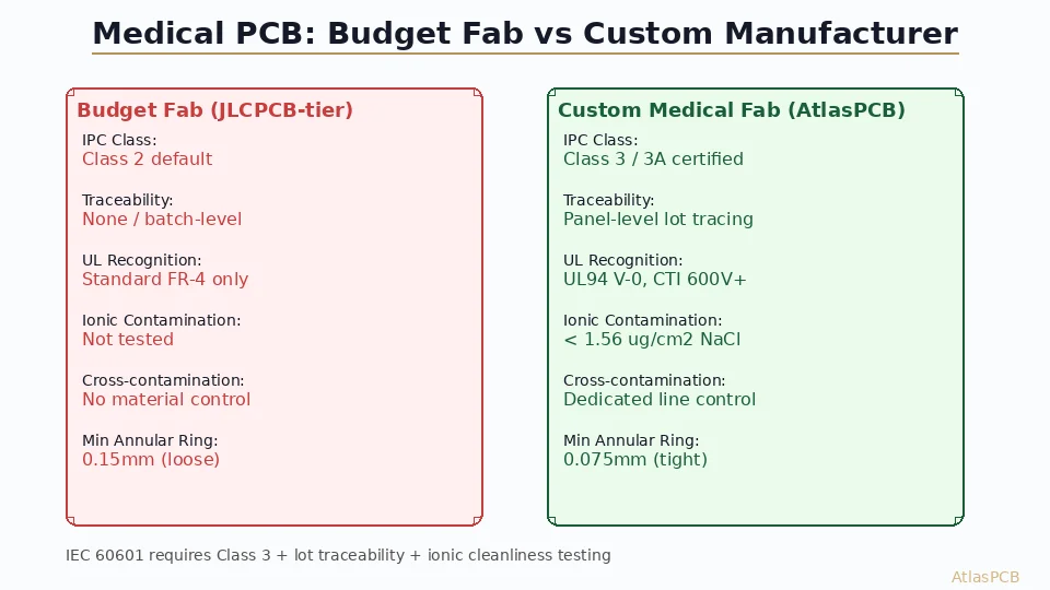
Quick Answer: Budget Fabs Fail Medical on Process Control, Not Capability
| Requirement | JLCPCB / Budget Fab | Custom Medical Manufacturer |
|---|---|---|
| IPC Class | Class 2 (default) | Class 3 certified |
| Material Traceability | Batch-level, no CoC | Panel-level with full CoC chain |
| Ionic Cleanliness | Not tested | Tested per IPC-TM-650 2.3.25 |
| UL Recognition | Standard FR-4 only | UL94 V-0, CTI 600V+ documented |
| Cross-Contamination | Multi-customer shared lines | Dedicated or controlled lines |
| Electrical Test | Statistical sampling | 100% continuity + isolation |
| Min Annular Ring | 0.15mm (IPC Class 2) | 0.075mm with Class 3 verification |
| Documentation | None | Device History Record support |
The gap is not about whether a budget fab can make a 4-layer board with your trace widths. They absolutely can. The gap is in everything that happens around the fabrication: how materials are verified, how processes are controlled, how defects are caught, and how all of it is documented.
The IEC 60601 Compliance Problem
Engineers building medical devices often start prototyping on JLCPCB because it is fast, cheap, and the boards work electrically. The design validates, the firmware runs, the sensors read correctly. So the natural question becomes: why pay 5x more for the “same” board from a medical-qualified manufacturer?
The answer lies in what IEC 60601-1 actually demands from the complete device, and how those demands flow down to PCB fabrication. Section 8.9 specifies creepage and clearance distances between conductors at different voltage levels — distances that must be maintained not just in the design files but on the physical board, accounting for registration tolerance, etching variation, and solder mask misalignment. A budget fab running Class 2 tolerances can easily eat into your safety margins. In our DFM reviews for medical customers, we routinely find that boards designed with exactly the IEC 60601 minimum creepage distance violate that minimum once you account for the +/-3 mil registration tolerance typical of budget services.
Section 11 addresses temperature limits, which means the PCB material must have documented thermal properties — glass transition temperature, decomposition temperature, and coefficient of thermal expansion — backed by material certificates from the laminate supplier. Budget fabs use whatever FR-4 is cheapest that week. They do not provide material certificates because they do not track which specific laminate lot went into your panel. For a medical device that undergoes autoclave sterilization at 134 degrees Celsius, you need to know your FR-4 has a Tg above 150C and that this is verified per lot, not assumed from a generic datasheet.
MEDICAL DEVICE PCB
Need IEC 60601-Compliant Boards?
AtlasPCB fabricates Class 3 medical PCBs with full material traceability and ionic cleanliness testing. We support FDA DHR documentation requirements.
Get Medical PCB Quote ›
Where Budget Fabs Structurally Fail
Material Sourcing and Documentation
A medical PCB manufacturer maintains a qualified supplier list (QSL) for laminates, prepreg, copper foil, and surface finish chemicals. Each incoming material shipment is verified against a Certificate of Conformance from the laminate supplier — documents like Isola’s CoC that specify the exact lot number, Dk, Df, Tg, and CTE values measured on that production run. This creates the traceability chain that FDA auditors follow during 21 CFR 820 inspections.
Budget fab services purchase materials opportunistically. They might use Shengyi S1000-2 one week and Kingboard KB6160 the next, depending on price and availability. Both are legitimate FR-4 laminates, but they have different dielectric constants (4.2 vs 4.4 at 1 GHz), different Tg values (150C vs 170C), and different CTI ratings. For your medical device, this variability is unacceptable — your EMC certification was validated with specific dielectric properties, and your safety analysis assumed a specific CTI rating for creepage distance calculations.
Ionic Contamination Control
IPC-TM-650 Method 2.3.25 specifies the ROSE (Resistivity of Solvent Extract) test for ionic cleanliness. Medical devices that contact patients or operate in sterile environments must demonstrate ionic contamination below 1.56 micrograms per square centimeter NaCl equivalent. Some OEMs set even tighter limits at 0.75 ug/cm2 for implantable devices.
Budget fabs do not test for ionic cleanliness. Their process lines handle hundreds of different customers’ boards simultaneously, with no controlled cleaning between jobs. Flux residues from one customer’s solder mask process can contaminate the next customer’s bare boards. In our facility, medical orders run on cleaned lines with monitored DI water rinse stages and post-fabrication ROSE testing on every production lot.
Electrical Testing Coverage
IPC-9252 defines three levels of electrical testing: fixture test (100% nets), flying probe (100% nets, slower), and statistical sampling. Budget services use statistical sampling or fixture test with a margin — they verify continuity and isolation but accept a defect escape rate of 50-100 ppm (parts per million). That might be acceptable for consumer electronics, but a medical device with 2000 nets has a meaningful probability of shipping with an open via or a near-short that was not caught.
At AtlasPCB, medical orders receive 100% flying probe testing with tightened isolation thresholds (typically 200 MOhm versus the standard 10 MOhm), catching not just hard shorts but degraded insulation resistance that indicates contamination or partial delamination.
FREE DFM REVIEW
Upload Your Medical Device Gerbers
Our engineers review creepage/clearance compliance, material compatibility, and IPC Class 3 manufacturability before quoting.
Real Failure Modes We See from Budget-Fab Medical Boards
Case 1: Creepage Violation After Solder Mask Misalignment
A customer brought us a redesign project after their patient monitoring device failed UL 60601 testing. The design had 6.4mm creepage between mains-connected traces and SELV circuits — exactly meeting the 6.4mm minimum for 250V working. Their JLCPCB boards showed solder mask misalignment of 4 mil, exposing copper at trace edges and reducing effective creepage to 5.9mm. The UL test engineer caught it. Our production boards hold solder mask registration to +/-2 mil with 100% optical verification.
Case 2: Autoclave-Induced Delamination
An endoscope OEM experienced board delamination after 50 autoclave cycles at 134C. Investigation revealed the budget fab had used standard-Tg FR-4 (Tg 135C) instead of the specified high-Tg material (Tg 170C). Since no material certificates accompanied the boards, the OEM had no evidence the specification was violated until boards failed in the field. With traceable material sourcing, this failure is caught at incoming inspection — the CoC proves which laminate was used.
Case 3: Electrochemical Migration from Ionic Contamination
A wearable glucose monitor experienced intermittent readings after 6 months. Root cause: ionic contamination from inadequately cleaned flux residues created electrochemical migration paths between sense electrodes at 3.3V differential under humid body-contact conditions. The budget-fab boards measured 3.8 ug/cm2 NaCl equivalent — above the 1.56 ug/cm2 threshold. Production boards from a controlled process measured 0.4 ug/cm2.
RELIABILITY TESTING
Verify Your Medical PCB Meets IPC Class 3
Our process includes ionic cleanliness testing, thermal stress verification, and microsection analysis — standard on every medical order.
View Our Process ›When Budget Fabs Are Acceptable for Medical Projects
Not every medical-adjacent project requires a fully qualified manufacturer from day one. Here is a realistic decision framework:
Concept Validation (OK to use budget fab): You are testing whether the circuit works at all — sensor accuracy, algorithm validation, power consumption measurement. The board will never see patients, never enter a clinical environment, and never be submitted to a notified body. Save the money here.
Design Verification (switch to qualified fab): Once you are building units for formal V&V testing — especially EMC testing to IEC 60601-1-2 — you need boards from the production process. EMC results are only valid if the board materials and construction match production intent. Testing on budget-fab boards and then switching manufacturers invalidates your test data.
Design Transfer and Production (must use qualified fab): At this stage, you need full DHR documentation, lot traceability, and all process controls active. This is not negotiable — 21 CFR 820.184 requires device history records that trace all components to their source.
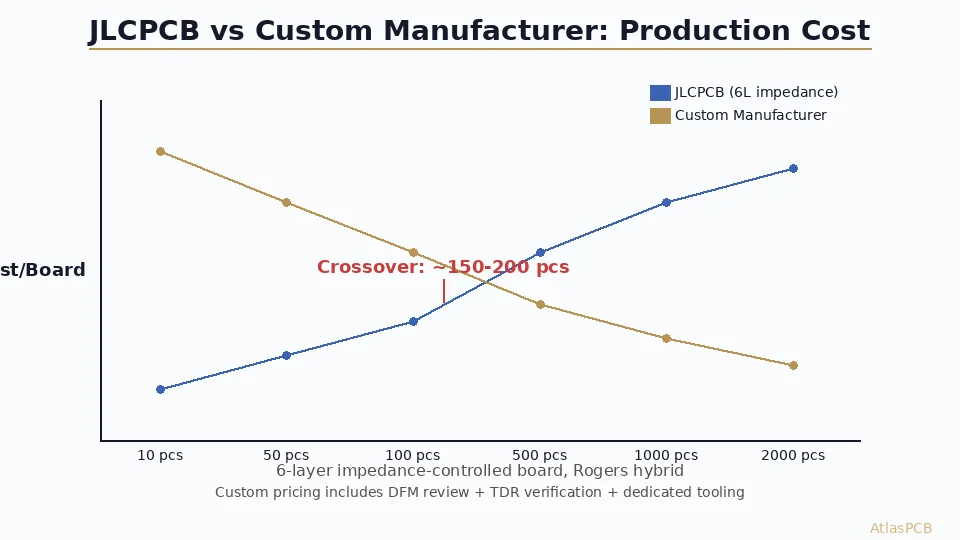
The cost of re-testing after switching manufacturers at the wrong stage typically exceeds the savings from using a budget fab during prototyping. In our experience supporting medical startups, the break-even point for switching to qualified fabrication is the design verification stage — usually 20-50 boards.
Cost Comparison: True Total Cost of Ownership
| Factor | JLCPCB (100 pcs, 4L) | Custom Medical (100 pcs, 4L) |
|---|---|---|
| Board fabrication | $500-800 | $2,000-3,500 |
| Material certificates | Not available | Included |
| Ionic cleanliness test | Not available | Included |
| 100% electrical test | Statistical sampling | 100% flying probe |
| Lot traceability | Batch only | Panel-level |
| Failed UL/IEC test rework | $15,000-50,000 risk | Minimal risk |
| Re-testing if supplier change | $20,000-80,000 risk | N/A (same supplier) |
| Total cost of ownership | $500-800 + $35,000-130,000 risk | $2,000-3,500 |
The budget fab looks cheap until you account for the cost of a failed compliance test that requires re-fabrication and re-testing. A single failed EMC or safety test costs more than a year of medical-grade fabrication.
ATLASPCB
Ready to Qualify Your Medical Device PCB?
Upload your Gerbers for a medical-grade quote with IPC Class 3 process control, full material traceability, and ionic cleanliness testing included.
Get Medical PCB Quote ›
Reviewed by AtlasPCB Engineering Team — 15+ years in advanced PCB fabrication for RF, HDI, and rigid-flex applications.
Related Reading:
About AtlasPCB — We specialize in complex PCB manufacturing for HDI, RF, and high-reliability applications. Explore our full PCB manufacturing capabilities, or get an instant online quote . Every order includes free engineering review. Get your quote.
Reviewed by AtlasPCB Engineering Team — IPC-certified manufacturing specialists with 15+ years of production experience in HDI, RF, and high-reliability PCB fabrication. Content based on factory floor data and real customer design reviews.
Frequently Asked Questions
Can I use JLCPCB for medical device prototypes?
What specific IEC 60601 requirements affect PCB fabrication?
How much more does a medical-grade PCB cost versus JLCPCB?
What certifications should a medical PCB manufacturer have?
What is the difference between IPC Class 2 and Class 3 for medical devices?
- JLCPCB vs custom PCB manufacturer
- medical device PCB requirements
- IEC 60601
- PCB manufacturer