· AtlasPCB Engineering · Engineering · 10 min read
HDI PCB Cost Breakdown 2026: 1+N+1 vs 2+N+2 vs 3+N+3 Pricing Guide
Detailed cost analysis of HDI PCB buildup options for 2026. Compares 1+N+1, 2+N+2, 3+N+3, and ELIC constructions with real pricing data, explains the cost drivers behind each sequential lamination cycle, and helps buyers optimize their HDI design for budget without sacrificing routing capability.
Quick Answer
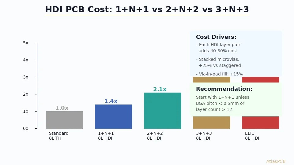
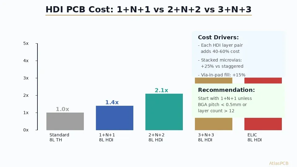
HDI PCB costs scale non-linearly with buildup complexity: 1+N+1 adds 35-50% over standard through-hole construction, 2+N+2 adds 100-120%, and 3+N+3 adds 200-250%. The cost drivers are sequential lamination cycles (each adds a full press/drill/plate/image cycle), microvia drilling (laser time + panel registration), and via fill requirements (copper or resin fill for stacked vias). For most 0.5mm-pitch BGA designs, 1+N+1 provides adequate breakout; 2+N+2 becomes necessary only for 0.4mm-pitch or finer, and 3+N+3 is reserved for 0.3mm-pitch CSP packages or extreme routing density requirements.
Quick Answer: HDI Cost by Buildup Type (2026 Q3 Pricing)
| Construction | Cost Multiplier | Typical Use Case | BGA Pitch Support |
|---|---|---|---|
| Standard 8L TH | 1.0x (baseline) | 0.8mm+ pitch, moderate routing | 0.8mm+ |
| 1+N+1 (8L HDI) | 1.4-1.5x | 0.5mm pitch BGA breakout | 0.5mm |
| 2+N+2 (8L HDI) | 2.1-2.3x | 0.4mm pitch, high pin-count | 0.4mm |
| 3+N+3 (8L HDI) | 3.2-3.5x | 0.3mm pitch CSP, max density | 0.3mm |
| ELIC (8L) | 4.5-5.0x | Smartphone/SiP, any-layer via | <0.3mm |
Real dollar amounts (8L, 100x80mm, qty 50, 10-day lead time):
- Standard TH: $12-18/board
- 1+N+1: $18-28/board
- 2+N+2: $28-42/board
- 3+N+3: $42-60/board
- ELIC: $58-85/board
These prices reflect July 2026 market conditions, including the 15-20% material cost increase driven by AI server demand absorbing high-end laminate supply. Prices are for Isola 370HR or Shengyi S1000-2M with ENIG finish.
Understanding the Cost Drivers
HDI PCB pricing is not simply “more layers = more cost.” The cost structure is dominated by sequential processing — each HDI buildup pair adds an entire manufacturing cycle that must be completed before the next pair begins. Understanding what drives each cost element helps you optimize your design for budget without sacrificing the routing density you actually need.
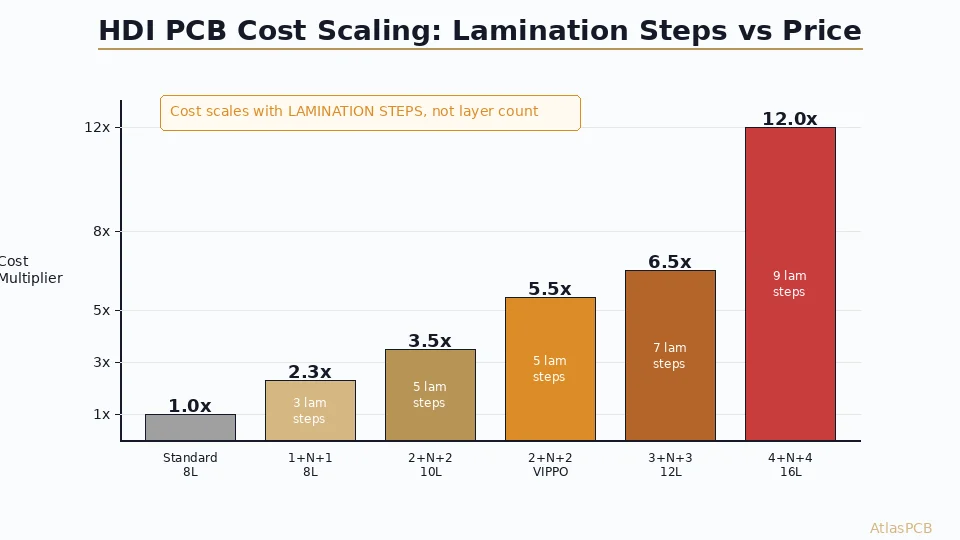
The single largest cost driver is the number of sequential lamination cycles. A standard multilayer board, regardless of layer count, goes through one lamination press cycle: all layers are stacked and bonded simultaneously. A 1+N+1 HDI board requires three press cycles — one for the core, then one each for the top and bottom buildup layers. A 2+N+2 requires five press cycles. Each press cycle takes 3-4 hours of actual press time plus 2-3 hours of layup preparation and post-press inspection. That’s 5-7 hours of production capacity per cycle, multiplied across however many panels your order requires.
The second major driver is laser drilling. Every microvia requires a discrete laser hit — a UV or CO2 laser pulse precisely positioned to ablate through one dielectric layer and stop on the copper target pad below. Our facility runs Hitachi UV-YAG laser drills capable of 50,000 holes per hour at 0.1mm diameter. A typical HDI panel with 400 boards might contain 2-4 million microvias, requiring 40-80 hours of laser drill time per panel. Compare this to mechanical drilling, which drills all layers simultaneously in one pass at 150,000 holes per hour. The laser time alone accounts for 20-30% of the HDI cost premium.
The third factor is via fill — either resin or copper. For stacked microvia constructions (where a microvia on Layer 1-2 must have another microvia stacked directly on top of it from Layer 2-3), the bottom via must be filled and planarized flat before the next buildup layer can be laminated. Copper fill provides better thermal and electrical performance but requires multiple plating cycles and mechanical planarization. Resin fill is cheaper but has higher thermal resistance and cannot carry current. In our experience, roughly 60% of HDI designs require copper fill for at least some vias (typically under BGA thermal pads), adding the VIPPO process step.
HDI PCB MANUFACTURER
Get an HDI PCB Quote in 4 Hours
We manufacture 1+N+1 through 5+N+5 HDI with stacked or staggered microvias, VIPPO, and via-in-pad. Upload your design for accurate pricing based on your actual construction.
Upload Gerber Files ›
1+N+1: The Sweet Spot for Most Designs
For the majority of HDI applications — particularly those driven by a single high-pin-count BGA at 0.5mm pitch — 1+N+1 construction provides the optimal balance of routing density and cost. One microvia layer on each side of the board is sufficient to break out the outer two rows of a 0.5mm-pitch BGA array, routing them to inner layers through blind microvias while the interior pins escape through standard through-hole vias.
The cost premium of 35-50% over standard through-hole construction buys you: laser-drilled blind vias (typically 0.1mm diameter, 0.35mm capture pad) on the outer layers, one additional lamination cycle per side, and the registration accuracy needed to land microvias on their target pads (typically +/-25 um layer-to-layer). What you don’t get is the ability to stack vias (because there’s only one microvia layer) or route all signal layers with microvias (inner layers still use through-hole vias).
In practice, 1+N+1 allows you to reduce total layer count by 2 compared to an equivalent through-hole design. A routing challenge that would require 10 layers with conventional through-hole vias can often be solved in 8 layers with 1+N+1 HDI — because the blind microvias don’t create routing blockages on inner layers the way through-hole vias do. This layer reduction partially offsets the HDI cost premium: an 8-layer 1+N+1 board might cost similar to a 10-layer through-hole board while providing better signal integrity (shorter via stubs).
Based on our production data from Q2 2026, 1+N+1 represents approximately 45% of all HDI orders we process — making it by far the most common HDI construction type. The typical customer is designing a product with one or two large BGA components (FPGA, SoC, or application processor) at 0.5mm pitch surrounded by standard 0.65-0.8mm pitch peripherals that don’t require HDI. The microvias serve the large BGA; everything else uses conventional vias.
2+N+2: When 0.4mm Pitch Demands More
The jump from 1+N+1 to 2+N+2 is the largest proportional cost increase in the HDI spectrum — roughly doubling the board cost from 1.4x to 2.1x baseline. This steep increase reflects the addition of a second sequential lamination cycle (with its associated laser drilling, imaging, and plating steps) plus the via fill requirement that comes with stacking two microvia layers.
The engineering justification for 2+N+2 is straightforward: you need it when your BGA pitch drops below 0.5mm or when the pin count exceeds what one microvia layer can physically break out. At 0.4mm pitch, the pad-to-pad spacing between BGA balls is only 150-170 um after landing pad geometry is subtracted. A single microvia layer provides one routing channel between pads — sufficient for the outer 2-3 rows but insufficient for interior pins on a large array.
With 2+N+2, you get two microvia layers per side, allowing the outer row to escape on Layer 1-2, the next row on Layer 2-3, and deeper pins through the now-accessible inner routing layers. This effectively doubles your breakout capacity without increasing the board’s overall layer count.
The stacked versus staggered microvia decision becomes critical at 2+N+2. Stacked microvias (directly aligned on top of each other) provide the minimum pad size and maximum routing density, but require copper fill of the first via before the second is drilled on top. This fill process adds $2-5/board at production volumes. Staggered microvias (offset by 0.2-0.3mm) avoid the fill requirement but consume more routing space due to the offset landing pads. In our production mix, approximately 70% of 2+N+2 boards use stacked microvias with copper fill — the density advantage typically justifies the cost premium for the type of designs that need 2+N+2 in the first place.
DESIGN OPTIMIZATION
Can Your Design Work with Less HDI?
Our engineers review your BGA fanout and routing density to determine the minimum HDI construction that meets your requirements. Many 2+N+2 designs can be optimized down to 1+N+1 with routing changes.
Request Design Review ›Cost Optimization Strategies That Actually Work
Having processed over 3,000 HDI orders in the past year, our engineering team has identified several design choices that significantly reduce HDI cost without compromising functionality:
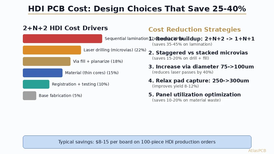
1. Use staggered microvias where stacking isn’t required. Not every via needs to stack. If your microvia on Layer 1-2 connects to a trace on Layer 2 that routes to a different location before dropping to Layer 3, that Layer 2-3 via can be staggered. Eliminating copper fill on even 30% of your microvias saves 4-6% on the total board cost.
2. Minimize the HDI region. If only one area of your board has 0.5mm-pitch BGAs and the rest is 0.8mm+ pitch, consider a design where only the BGA region uses HDI fanout while the rest of the board uses standard through-hole vias. Some manufacturers (including our facility) can accommodate regional HDI — where laser drilling is restricted to a defined zone — at reduced cost compared to full-panel HDI.
3. Choose the right via fill for each location. Copper fill (VIPPO) is necessary only for vias that serve as thermal paths for high-power BGAs or as stacking targets for the next microvia layer. Resin fill with cap plate is adequate for blind vias under standard SMD pads. Mixed fill strategies (copper in thermal via arrays, resin elsewhere) save 8-12% compared to blanket VIPPO.
4. Consider 1+N+1 with selective through-hole vias for center pins. For moderate-pin-count BGAs (200-400 balls at 0.5mm pitch), the outer 3-4 rows can escape through microvias while center pins use standard through-hole vias. This hybrid approach often eliminates the need for 2+N+2 construction — saving 40-50% of the cost premium.
5. Optimize panel utilization. HDI cost is heavily driven by fixed per-panel processing costs (each lamination, laser drill, and imaging cycle has a per-panel floor price). Maximizing the number of boards per panel — through panelization optimization, board outline nesting, or combining multiple designs on one panel — amortizes these fixed costs across more units. We offer panelization optimization as part of our DFM review at no additional charge.
Volume Pricing and Lead Time Impact
The HDI cost premium is not constant across order quantities — it compresses at higher volumes due to fixed-cost amortization and process optimization. Here’s how pricing scales for an 8-layer 2+N+2 board (100x80mm) in 2026:
| Quantity | Per-Board Cost | Effective Multiplier |
|---|---|---|
| 5 pcs (prototype) | $85-120 | 5-6x baseline |
| 50 pcs (pilot) | $28-42 | 2.1-2.3x |
| 500 pcs (low volume) | $18-25 | 1.5-1.8x |
| 5,000 pcs (production) | $12-16 | 1.0-1.2x |
| 50,000 pcs (mass) | $8-11 | 0.7-0.9x |
At prototype quantities, the multiplier is extreme because you’re paying for full panel setup, laser programming, test coupon design, and first-article inspection amortized across just 5 boards. At production volumes, these fixed costs become negligible per unit, and the HDI premium shrinks to mainly the material and laser drill time difference.
Lead time impact: 1+N+1 adds 2-3 days to standard lead time. 2+N+2 adds 4-6 days. 3+N+3 adds 7-10 days. These additions are irreducible — they represent the physical lamination, drilling, and plating cycles that cannot be parallelized. Rush orders for HDI are possible but expensive (50-80% premium) because they require displacing other work from the sequential process queue.
ATLASPCB
Get Accurate HDI Pricing for Your Design
Upload your Gerber files and let our system generate an instant quote based on your actual layer count, HDI construction, via types, and quantity. No guesswork — real pricing from our production floor.
Get Instant Quote ›
Reviewed by AtlasPCB Engineering Team — 15+ years in advanced PCB fabrication for RF, HDI, and rigid-flex applications.
Related Reading:
About AtlasPCB — We specialize in complex PCB manufacturing for HDI, RF, and high-reliability applications. Explore our HDI PCB manufacturing capabilities, impedance-controlled PCB manufacturing, or get an instant online PCB quote . Every order includes free engineering review. Get your quote.
Reviewed by AtlasPCB Engineering Team — IPC-certified manufacturing specialists with 15+ years of production experience in HDI, RF, and high-reliability PCB fabrication. Content based on factory floor data and real customer design reviews.
Frequently Asked Questions
How much more does HDI PCB cost compared to standard PCB?
When do I need 2+N+2 HDI instead of 1+N+1?
What is the cheapest way to build an HDI PCB?
Does via-in-pad add cost to HDI PCB?
How many layers do I actually need for HDI?
- HDI PCB manufacturer
- multilayer PCB cost
- PCB stackup design guide
- impedance controlled PCB manufacturer