· AtlasPCB Engineering · Engineering · 11 min read
AI Datacenter PCB Design: 112G PAM4 SerDes Routing and Thermal Management for GPU Baseboard
PCB design and manufacturing requirements for next-generation AI accelerator baseboards carrying 112G PAM4 SerDes channels. Covers material selection (Megtron 6/7 vs ultra-low-loss), stackup architecture for 20-30 layer boards, backdrill specifications, thermal via arrays for 500W+ TDP, and the manufacturing constraints that determine whether your AI hardware PCB is fabricable at volume.
Quick Answer
AI datacenter baseboard PCBs carrying 112G PAM4 SerDes require ultra-low-loss laminates (Df < 0.003 at 28 GHz), 20-30 layer stackups with 85-ohm differential impedance at +/-5% tolerance, backdrill stub residuals below 5 mil, and thermal via arrays capable of dissipating 500-1000W from GPU/ASIC packages. The fabrication complexity demands an HDI PCB manufacturer with controlled impedance capability, precision backdrilling, and sequential lamination — effectively limiting the supply base to a handful of qualified shops globally.
Quick Answer: 112G PAM4 PCB Manufacturing Requirements
| Parameter | Requirement | Why It Matters |
|---|---|---|
| Dielectric loss (Df) | < 0.003 @ 28 GHz | Each 0.001 Df = ~0.5 dB/inch additional loss |
| Impedance | 85 ohm diff, +/-5% | PAM4 eye closure from reflections |
| Backdrill stub | < 5 mil residual | Stub resonance at 28 GHz = 2 dB/via |
| Trace/space | 3.5/3.5 mil minimum | BGA breakout for 0.8mm pitch |
| Layer count | 20-30 layers | Signal + reference + power layers |
| Copper roughness | HVLP or UHVLP (Rz < 3 um) | Surface roughness adds 0.5+ dB/inch at 28 GHz |
| Via aspect ratio | 12:1 to 16:1 | 0.25mm drill through 4mm board |
| Board thickness | 3.5-5.0 mm | Accommodates 20-30 layers with proper dielectric spacing |
These specifications place AI datacenter PCBs at the absolute frontier of PCB manufacturing capability. Only manufacturers with advanced HDI processes, precision backdrilling, and ultra-low-loss material processing experience can reliably produce these boards.
The 112G Signal Integrity Challenge
The move from 56G NRZ to 112G PAM4 did not simply double the data rate — it fundamentally changed what the PCB must deliver. NRZ signaling has two voltage levels with 20 dB of vertical eye opening; PAM4 has four levels with only 9.5 dB between adjacent levels. This 10.5 dB penalty means every source of signal degradation that was tolerable at 56G becomes critical at 112G.
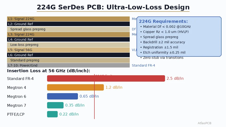
Consider insertion loss: a 6-inch differential pair on standard FR-4 at 28 GHz (the Nyquist frequency for 112G PAM4) loses approximately 12 dB. With a total channel budget of 28-32 dB (depending on the transceiver technology), a 6-inch trace consumes nearly half your budget before accounting for connectors, via transitions, packages, and crosstalk. This is why ultra-low-loss materials became mandatory rather than optional — Megtron 6 reduces that same trace loss to roughly 4.5 dB, preserving budget for the other loss contributors.
The challenge compounds with copper surface roughness. Standard electrodeposited (ED) copper has an Rz roughness of 5-8 um. At 28 GHz, the skin depth is approximately 0.4 um, meaning the signal current flows entirely within the roughness features. The Huray snowball model shows this adds 30-40% additional conductor loss on standard copper versus smooth alternatives. HVLP (Hyper Very Low Profile) copper at Rz < 3 um reduces this penalty to 10-15%, and UHVLP at Rz < 1.5 um brings it below 5%.
In our facility, we process Megtron 6 and Megtron 7 with HVLP copper as standard for high-speed designs. The combination delivers consistent insertion loss of 0.6-0.8 dB/inch at 28 GHz for edge-coupled stripline — within the budget required for 112G PAM4 channels up to 8-10 inches between breakout points.
HIGH-SPEED PCB
112G PAM4 Capable PCB Fabrication
AtlasPCB processes Megtron 6, Megtron 7, and EM-890 with HVLP copper. Up to 30 layers with +/-5% impedance control and precision backdrilling.
Get High-Speed PCB Quote ›
Stackup Architecture for AI Baseboard
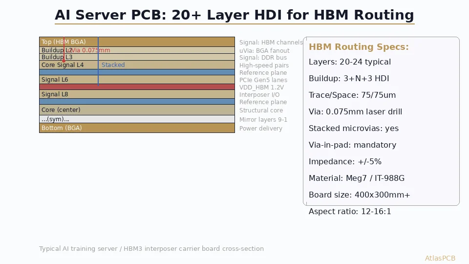
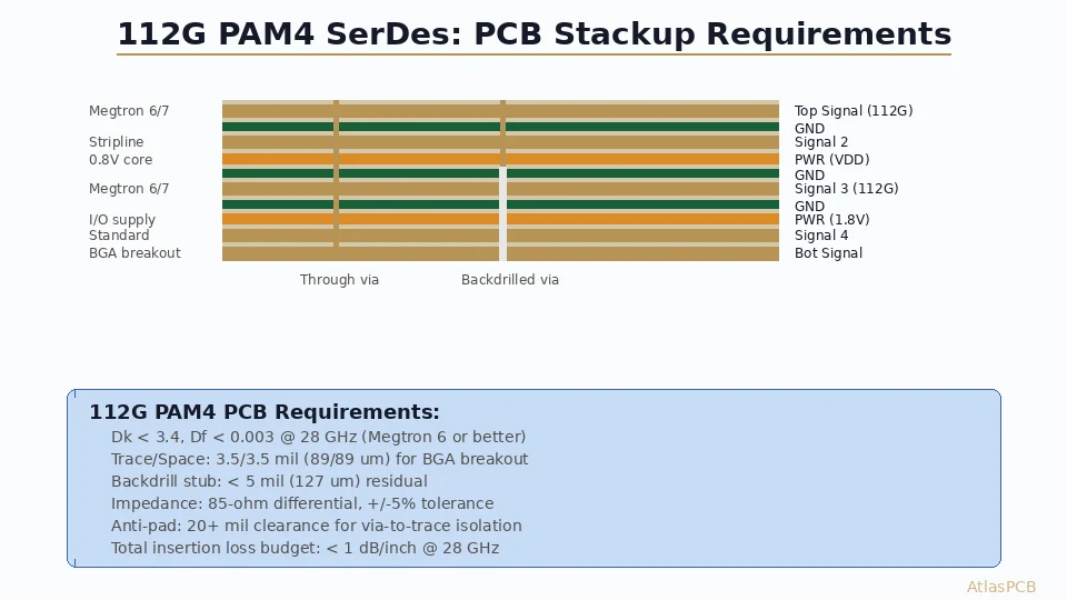
A representative 24-layer stackup for an AI GPU baseboard illustrates the engineering tradeoffs:
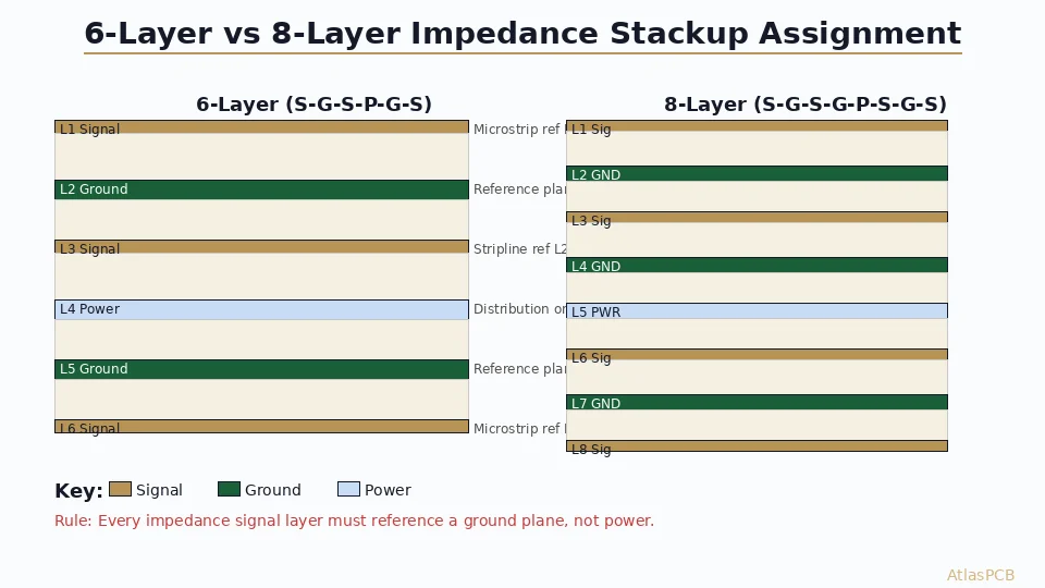
Layers 1-2: Top signal + adjacent ground. Microstrip breakout from GPU BGA (0.8mm pitch, requiring 3.5/3.5 mil trace/space for routing escape). Material: Megtron 6, 4 mil dielectric to ground reference.
Layers 3-6: Two signal layers with ground references. Edge-coupled stripline for 112G SerDes differential pairs. 85-ohm differential impedance, 3.8 mil trace width, 5 mil spacing within pair, 20+ mil pair-to-pair spacing for crosstalk isolation. Material: Megtron 6 for signal dielectrics.
Layers 7-10: Power distribution. Multiple voltage islands (0.75V GPU core, 0.85V HBM, 1.2V miscellaneous, 1.8V I/O). Heavy copper (2 oz) for current handling — a 700W GPU at 0.75V draws 930A, requiring wide copper planes with controlled impedance paths from VRM to die.
Layers 11-14: Additional signal layers for DDR5/HBM interposer routing, I2C/SPI management buses, and PCIe Gen5 interconnects. These layers use standard mid-loss material (Megtron 4 or equivalent) since the signals operate at lower frequencies (up to 16 GT/s for PCIe Gen5 versus 112 Gbps for SerDes).
Layers 15-18: Mirror of power distribution for the bottom-side power supply routing and additional ground layers for EMI containment.
Layers 19-24: Bottom signal layers and BGA breakout for secondary components (BMC, NVSwitch, memory controllers). Same Megtron 6 requirement for any 112G signals; mid-loss acceptable for slower interfaces.
The hybrid material approach — Megtron 6/7 for high-speed signal layers and Megtron 4 or standard FR-4 for power/ground — reduces material cost by 25-35% versus all-Megtron-6 construction while maintaining signal integrity where it matters. However, this hybrid approach requires careful CTE matching and press cycle optimization to prevent delamination at the material interfaces. We validate hybrid stackups through thermal cycling qualification (288 reflow cycles per IPC-9701) before committing to production.
Backdrill: The Most Critical Manufacturing Step
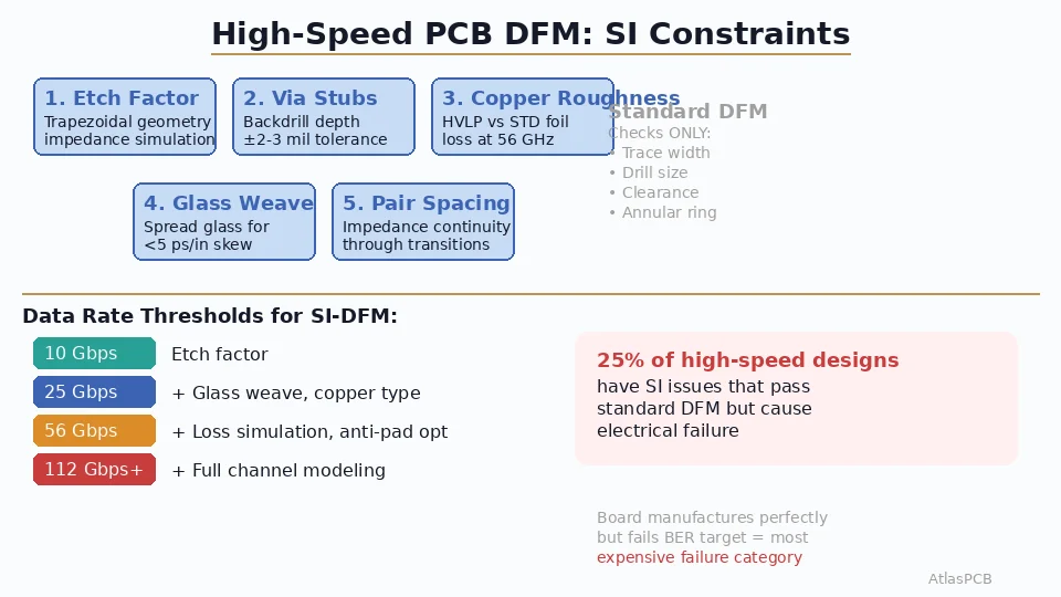
For 112G PAM4 via transitions, the backdrill specification determines whether the channel meets its loss budget or fails. The physics are simple: a via stub acts as a quarter-wave resonant stub. A 15-mil stub resonates at approximately 24 GHz in Megtron 6 (effective Dk ~3.6). This resonance frequency sits directly in the signal band for 112G PAM4, creating a notch that can absorb 3-5 dB of signal energy.
The backdrill process uses a larger-diameter drill bit (typically 0.35-0.40mm, versus 0.25-0.30mm for the signal via) aligned by X-ray registration to the existing via position, then drilled from the back side to within a controlled distance of the signal layer connection. The residual stub — what remains after drilling — must be less than 5 mil (127 um) for 112G applications.
Achieving 5-mil residual consistently across a production panel requires: X-ray alignment accuracy of +/-1 mil (for drill positioning), drill depth control of +/-2 mil (for stub length), and panel thickness uniformity within +/-2 mil (since the drill references from the panel surface). Any variation in panel thickness directly adds to stub length variation.
In our production, we run 100% X-ray inspection of backdrilled vias on 112G boards, verifying both the drill position (must be concentric with the original via within 2 mil) and the residual stub length (measured by cross-section on coupon vias, one per panel minimum). Boards that exceed the 5-mil specification are scrapped — we do not attempt to re-drill, as the additional mechanical stress risks damaging the plated barrel.
PRECISION BACKDRILL
+/-3 mil Backdrill Accuracy for High-Speed Channels
X-ray aligned backdrilling with 100% inspection. Verified by cross-section on every production panel. Supports 112G PAM4 stub requirements.
Thermal Management: 500-1000W Through a PCB
AI accelerators are pushing single-package TDP to extraordinary levels — NVIDIA’s B200 dissipates 1000W, AMD’s MI300X reaches 750W, and even inference chips like Groq’s LPU hit 300W. This thermal energy must be extracted through some combination of top-side heatsinking (through thermal interface material to the package lid) and bottom-side extraction (through the PCB to a cold plate in server architectures that use direct-to-board liquid cooling).
The PCB’s role in thermal management centers on the thermal via array beneath high-power packages. Standard FR-4 has a through-plane thermal conductivity of 0.3 W/mK — essentially a thermal insulator. A via array transforms this: each filled copper via (diameter 0.3mm, copper fill) provides a local thermal conductivity of approximately 400 W/mK through its cross-section. An array of vias on 1mm pitch covering a 50x50mm die shadow area provides an effective through-board thermal conductivity of 15-25 W/mK — a 50-80x improvement over bare substrate.
Design rules for thermal via arrays in AI hardware:
Via diameter: 0.3mm finished hole (0.4mm drilled, plated and filled). Larger vias provide more copper cross-section but consume more routing real estate. The 0.3mm standard represents an optimized tradeoff for GPU baseboard applications.
Via pitch: 1.0mm center-to-center. Closer spacing (0.8mm) improves thermal performance by 20% but creates fabrication challenges — the annular ring becomes too small for reliable plating and filling at aggressive aspect ratios.
Fill material: Electroplated copper fill (VIPPO — Via-in-Pad Plated Over) provides the best thermal conductivity. Conductive paste fill (silver epoxy) is acceptable but has 3-5x lower conductivity (60-100 W/mK versus 400 W/mK for copper). Non-conductive paste fill is NOT acceptable for thermal vias — it provides minimal thermal benefit over unfilled vias.
Connection to planes: Every thermal via must connect to at least two internal copper planes (preferably all ground planes) to provide lateral heat spreading. The internal planes act as heat spreaders, distributing the thermal energy over a larger area before it reaches the cold plate attachment surface.
Manufacturing Supply Chain Constraints
The combination of ultra-low-loss materials, 20+ layer construction, precision backdrilling, and tight impedance control limits the global supply base for AI datacenter PCBs to perhaps 15-20 qualified manufacturers. The key bottleneck is not equipment (many fabs have LDI and precision drill capability) but process expertise and material relationships.
Megtron 6 and Megtron 7 laminates are produced exclusively by Panasonic, with allocation that heavily favors established high-volume customers. A manufacturer without an existing allocation agreement cannot simply order Megtron 6 and start production — lead times for non-allocated material stretch to 8-12 weeks. Similarly, EM-890 (from EMC/Lianmao) and TU-87P (from TUC/Taiwan Union Technology) have limited global production capacity that is largely spoken for by the major server OEMs.
For engineering teams designing AI hardware, the practical implication is clear: engage your PCB manufacturer during the design phase, not after Gerber release. The manufacturer’s material availability, stackup capability, and process constraints should inform your design choices — not the other way around. A stackup that looks optimal in simulation but requires a material the manufacturer cannot source in time is useless.
At AtlasPCB, we maintain stocked inventory of Megtron 6 in standard thickness configurations and have allocation agreements for Megtron 7 with 4-6 week material lead time. We engage early with AI hardware customers to align their stackup requirements with our material availability, often saving 3-4 weeks of schedule versus manufacturers who order material after receiving customer Gerbers.
HDI PCB MANUFACTURER
AI Hardware PCB Partner with Material Stock
Megtron 6 in stock, Megtron 7 on allocation. 20-30 layer capability with sequential lamination and precision backdrilling for 112G SerDes.
Discuss Your AI PCB Project ›Cost Expectations for AI Datacenter Boards
| Board Specification | Prototype (5-10 pcs) | Production (100+ pcs) |
|---|---|---|
| 24L Megtron 6, standard backdrill | $800-1,200/board | $350-550/board |
| 28L Megtron 6/7 hybrid, precision backdrill | $1,500-2,500/board | $600-900/board |
| 30L full Megtron 7, VIPPO thermal vias | $2,500-4,000/board | $900-1,400/board |
These are board-level costs for a typical 18”x24” (457x610mm) server baseboard panel containing 1-2 boards. The cost is dominated by material (35-45%), sequential lamination steps (20-25%), and backdrilling/inspection (15-20%). Volume pricing improves significantly at 500+ boards due to panel optimization and reduced per-unit testing overhead.
For reference: a standard 8-layer FR-4 board of similar size runs $40-80 per board in production. The AI board premium of 10-20x reflects the compounding of material cost (3-5x), layer count (2-3x), process complexity (2-3x), and tighter specifications requiring higher yield loss absorption.
ATLASPCB
Building Next-Gen AI Hardware? Start with the PCB.
Upload your stackup requirements or Gerbers for an AI-grade PCB quote. We support 112G PAM4 channels with Megtron 6/7, precision backdrilling, and thermal via arrays up to 30 layers.
Get AI Hardware PCB Quote ›
Reviewed by AtlasPCB Engineering Team — 15+ years in advanced PCB fabrication for RF, HDI, and rigid-flex applications.
Related Reading:
About AtlasPCB — We specialize in complex PCB manufacturing for HDI, RF, and high-reliability applications. Explore our HDI PCB manufacturing capabilities, RF and high-frequency PCB services, or get an impedance-controlled PCB manufacturing . Every order includes free engineering review. Get your quote.
Reviewed by AtlasPCB Engineering Team — IPC-certified manufacturing specialists with 15+ years of production experience in HDI, RF, and high-reliability PCB fabrication. Content based on factory floor data and real customer design reviews.
Frequently Asked Questions
What PCB material is required for 112G PAM4 SerDes?
How many layers does an AI GPU baseboard PCB need?
What impedance tolerance is needed for 112G channels?
What backdrill specification is needed for 112G SerDes vias?
How is thermal management handled on AI GPU baseboards?
- HDI PCB manufacturer
- RF PCB design and manufacturing
- PCB stackup design guide
- impedance controlled PCB manufacturer