· AtlasPCB Engineering · Engineering · 9 min read
5G Antenna PCB Fabrication: mmWave Array Material Selection and Stackup Design
Building 5G mmWave phased array antenna PCBs? Material selection, stackup architecture, via fence isolation, and fabrication tolerances for 24-77 GHz antenna arrays — from prototype through volume production.
Quick Answer
5G mmWave antenna PCBs (24-77 GHz) require Rogers or PTFE materials for the antenna/feed layers (Dk stability critical for beam steering accuracy), via fence ground isolation between elements (pitch < lambda/10), and tight thickness control (+/-0.5 mil) for impedance and radiation pattern conformance. Standard FR-4 is unsuitable above 10 GHz due to loss tangent and Dk variation that detunes patch elements by 200-500 MHz.
Quick Answer: 5G Antenna PCB Material Selection
| Frequency Band | Recommended Material | Key Parameters | Typical Antenna Type |
|---|---|---|---|
| Sub-6 GHz (3.5-4.9 GHz) | High-Tg FR-4 or Megtron 4 | Dk 3.8-4.0, Df 0.005-0.008 | Patch array, slot |
| 24-28 GHz (n257/n258/n261) | Rogers RO4350B | Dk 3.48, Df 0.0037 | Patch array, SIW |
| 37-40 GHz (n260) | Rogers RO4350B or RO3003 | Dk 3.0-3.48, Df 0.001-0.004 | Dense patch array |
| 57-71 GHz (WiGig) | RO3003 or LCP | Dk 2.9-3.0, Df 0.001 | Substrate-integrated |
| 76-81 GHz (automotive radar) | RO3003 or RT5880 | Dk 2.2-3.0, Df 0.0009-0.001 | Series-fed patch |
The manufacturing reality: Material selection is not just about electrical properties — it determines your fabrication options, cost, and lead time. RO4350B processes on standard FR-4 equipment. PTFE materials require specialized handling. Choose the material that gives acceptable RF performance while keeping your board manufacturable at target cost.
Why mmWave Antenna PCBs Are Different from Standard RF Boards
Designing a PCB antenna at 28 GHz is fundamentally different from designing a standard RF board at 2.4 GHz, and the fabrication requirements reflect this. At millimeter-wave frequencies, the PCB substrate is not just carrying signals — it is part of the radiating structure. The substrate thickness, dielectric constant, and copper geometry directly determine radiation efficiency, bandwidth, and beam pattern.
A 28 GHz patch antenna on RO4350B has physical dimensions of approximately 3.2 x 2.6 mm. At these dimensions, a 25 um (1 mil) error in patch width shifts the resonant frequency by 150-250 MHz. For a 5G NR channel with 400 MHz bandwidth, that shift moves the element passband partially outside the channel — reducing effective gain and distorting the array pattern. Compare this to a 2.4 GHz patch where the same 25 um error produces less than 5 MHz shift, well within any practical bandwidth.
The implication for PCB fabrication: antenna array PCBs require etch tolerance of +/-0.5 mil (12.7 um) across the entire array aperture — which may be 100-200mm. This is tighter than standard PCB manufacturing (typically +/-1.0 mil) and requires the manufacturer to characterize and compensate etch rate variation across the panel. In our facility, we achieve this through panel-level etch uniformity monitoring and compensation tables that adjust exposure dose based on position — a process we developed specifically for antenna array production.
The substrate thickness tolerance requirement is equally demanding. Standard multilayer PCB lamination holds thickness to approximately +/-2 mils across a panel. For antenna elements, we need +/-0.5 mil. This requires material pre-selection (measuring incoming laminate thickness and grouping panels by measured value) and press parameter optimization to minimize resin flow variation. We maintain a dedicated press program for antenna panels with tighter temperature ramp rates and longer soak times to achieve uniform flow.
CHINA RF PCB MANUFACTURER
mmWave Antenna PCB Fabrication Expertise
Rogers and PTFE material inventory in-house. Etch tolerance +/-0.5 mil for antenna elements. Via fence fabrication with pitch control for array isolation. Prototype to production volumes.
Get Antenna PCB Quote ›
Stackup Architecture for Phased Array Antennas
A practical 5G phased array antenna PCB is not a single-layer patch — it is a multi-layer structure integrating antenna elements, feed network, DC bias distribution, and often the beamforming IC connections. The stackup must separate these functions while maintaining controlled impedance on the feed network and providing solid ground reference planes for the antenna elements.
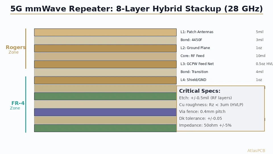
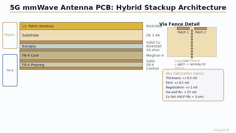
A typical 8-layer stackup for a 28 GHz 4x4 phased array might look like:
| Layer | Function | Material | Thickness | Notes |
|---|---|---|---|---|
| L1 | Patch antenna elements | RO4350B | - | Exposed copper, no soldermask over patches |
| Core 1-2 | Antenna substrate | RO4350B | 10 mil (0.254mm) | Critical: +/-0.5 mil tolerance |
| L2 | Ground plane | Copper | 0.5 oz | Solid, no routing — antenna reference |
| PP 2-3 | Isolation | RO4450F bondply | 4 mil | Bonds Rogers to FR-4 transition |
| L3 | Feed network | FR-4 (Megtron 4) | - | 50-ohm stripline, impedance controlled |
| Core 3-4 | Feed/digital separation | FR-4 Tg170 | 8 mil | - |
| L4 | Ground/power plane | Copper | 1 oz | DC distribution, digital ground |
| PP 4-5 | Standard | FR-4 prepreg | 4 mil | - |
| L5 | Digital control signals | FR-4 | - | SPI, I2C to beamformer ICs |
| Core 5-6 | Standard | FR-4 | 8 mil | - |
| L6 | Ground plane | Copper | 1 oz | Digital reference |
| PP 6-7 | Standard | FR-4 prepreg | 4 mil | - |
| L7 | Power distribution | FR-4 | - | VDD, VCC planes |
| Core 7-8 | Standard | FR-4 | 8 mil | - |
| L8 | Component/BGA side | FR-4 | - | Beamformer IC pads |
This hybrid stackup uses Rogers only for layers 1-2 where RF performance matters (antenna element and its ground reference), transitioning to FR-4 for the remaining structure. The RO4450F bondply at the transition interface is specifically designed for bonding Rogers to FR-4 in hybrid constructions, with compatible CTE and processing temperature.
The critical design rule: the antenna ground plane (L2) must be unbroken copper under the entire array aperture. Any slot, via antipads, or routing on L2 distorts the antenna ground reference and creates unpredictable radiation pattern distortion. All signal routing passes through lower layers via blind vias from L1 to L3 or beyond.
Via Fence Design for Element Isolation
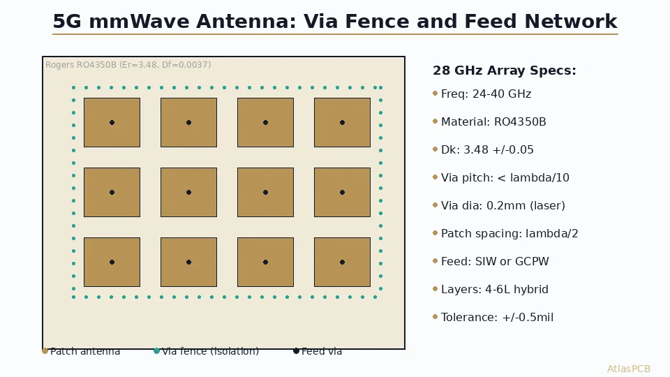
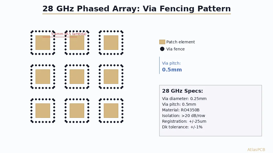
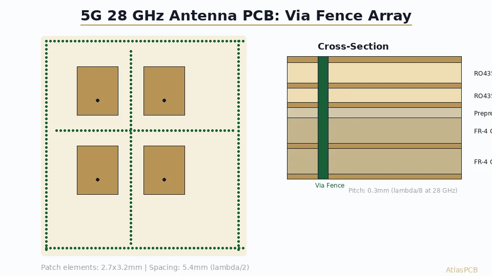
Surface waves are the primary coupling mechanism between adjacent antenna elements in an array. At 28 GHz on a 10-mil RO4350B substrate, the TM0 surface wave propagates along the dielectric interface and couples energy between patches spaced lambda/2 (approximately 5.4mm) apart. Without mitigation, mutual coupling between adjacent elements reaches -15 to -18 dB — enough to distort the array radiation pattern and reduce beam steering accuracy.
Via fences solve this by creating physical barriers to surface wave propagation. A row of plated through-holes connecting the top ground (around each patch) to the bottom ground plane creates a Faraday cage effect. For effective isolation at 28 GHz, the via pitch must be less than lambda/10 in the substrate (approximately 1.0mm for RO4350B with effective lambda accounting for Dk). Each via should be 0.3mm diameter minimum for reliable plating.
From our production experience with antenna arrays, the via fence implementation details that matter:
Via hole quality is more critical in antenna PCBs than standard boards. Rough or poorly plated via walls create discontinuities that reflect energy back toward the antenna element rather than conducting it to ground. We maintain via wall roughness below 25 um RMS for antenna boards, compared to the 50 um acceptable in standard PCBs. This requires fresher drill bits (shorter drill stacks) and optimized electroless/electrolytic plating chemistry.
The ground ring connecting via fence tops must be at least 0.3mm wide and have minimal clearance to the via antipad (0.1mm annular ring). Narrow ground rings create inductive sections that reduce isolation at higher harmonics. For 28 GHz fundamental with 56 GHz second harmonic, the ground ring acts as the current return path and must be low-impedance at both frequencies.
RF PCB DESIGN AND MANUFACTURING
Via Fence Fabrication with Tight Pitch Control
Minimum 0.15mm drill with 1.0mm pitch accuracy for mmWave via fences. Wall roughness controlled below 25 um RMS. Registration +/-1 mil for feed-to-patch alignment.
Copper Surface Roughness: The Hidden Performance Factor
At millimeter-wave frequencies, conductor loss often exceeds dielectric loss as the dominant loss mechanism. The skin depth at 28 GHz in copper is approximately 0.39 um — meaning current flows only in the outermost fraction of a micron of the copper surface. If that surface is rough, the effective current path length increases significantly, directly increasing resistive loss.
Standard electrodeposited (ED) copper foil has surface roughness (Rz) of 3-8 um on the tooth side (the side facing the dielectric). At 28 GHz, this roughness increases conductor loss by 50-100% compared to a smooth surface. For antenna elements where radiation efficiency directly determines array gain, this loss is unacceptable.
The solutions, in order of effectiveness and cost:
HVLP (Hyper Very Low Profile) copper has Rz of 1.5-3 um, reducing the roughness penalty to approximately 30-50% above ideal. This is the standard choice for 24-40 GHz antenna PCBs and adds minimal cost over standard foil — approximately 5-10% material premium.
Rolled annealed (RA) copper offers Rz below 1 um and is ideal for 60-77 GHz applications, but is only available bonded to flexible substrates (LCP, PTFE films). Its ultra-smooth surface minimizes conductor loss to within 15-20% of theoretical.
For our 5G antenna production, we stock RO4350B with HVLP copper as the default RF laminate. Orders specifying standard ED copper for mmWave antenna applications receive a DFM flag — we will fabricate it if requested, but we ensure the designer understands the efficiency impact before proceeding.
Prototype-to-Production Transition for Antenna Arrays
The transition from antenna prototype to volume production introduces challenges unique to array PCBs. A prototype that measures correctly on a single board may perform differently in production due to panel-level variations that did not appear on a single prototype panel.
The most common issue: etch uniformity varies across a production panel more than across a single prototype board. A prototype containing one array (say, 60x60mm) occupies a small region where etch rate is relatively uniform. Production panelization places multiple arrays across a 450x600mm panel, spanning regions with potentially different etch rates due to spray pattern, solution flow, and copper density variation. The result: arrays from the panel center measure on-target, while those near edges show 200-300 MHz resonant frequency shift.
Our approach for antenna production: we qualify the panel layout during the first production lot by measuring patch dimensions and TDR impedance at multiple panel positions (center, edge, corner). If position-dependent variation exceeds spec, we implement position-dependent exposure compensation — adjusting the imaging dose to pre-compensate for known etch variation. This panel mapping adds one engineering setup iteration but ensures all positions produce conforming arrays.
For teams transitioning from prototype to production, we recommend ordering a “pilot lot” of 5-10 panels before committing to full volume. This allows us to characterize panel uniformity, identify any position-dependent issues, and implement compensation before your main production run.
ATLASPCB
From Antenna Prototype to Production Array
Rogers and PTFE inventory. Tight etch and thickness for mmWave patch elements. Panel uniformity characterization for production consistency. 24-77 GHz proven capability.
Start Your Antenna Project ›
Reviewed by AtlasPCB Engineering Team — 15+ years in advanced PCB fabrication for RF, HDI, and rigid-flex applications.
Related Reading:
About AtlasPCB — We specialize in complex PCB manufacturing for HDI, RF, and high-reliability applications. Explore our RF and high-frequency PCB services, Rogers RO4350B PCB manufacturing, or get an multilayer PCB fabrication up to 30 layers . Every order includes free engineering review. Get your quote.
Reviewed by AtlasPCB Engineering Team — IPC-certified manufacturing specialists with 15+ years of production experience in HDI, RF, and high-reliability PCB fabrication. Content based on factory floor data and real customer design reviews.
Frequently Asked Questions
What PCB material is best for 5G mmWave antenna arrays?
How does PCB thickness tolerance affect antenna performance?
What is via fence isolation and why does it matter for antenna arrays?
Can I fabricate a 5G antenna PCB on FR-4?
What fabrication tolerances matter most for antenna PCBs?
- 5G antenna PCB fabrication
- RF PCB design and manufacturing
- Rogers 4350B stackup
- China RF PCB manufacturer
- mmWave PCB