· AtlasPCB Engineering · Engineering · 11 min read
5G 28 GHz Active Phased Array PCB: Thermal Via Design for Integrated PA Modules
Technical guide on PCB thermal management for 28 GHz 5G active phased array antennas with integrated power amplifiers. Covers thermal via array sizing, via pitch requirements for RF isolation, Rogers/FR-4 hybrid stackup thermal conductivity, and manufacturing considerations for high-density via arrays in millimeter-wave antenna substrates.
Quick Answer
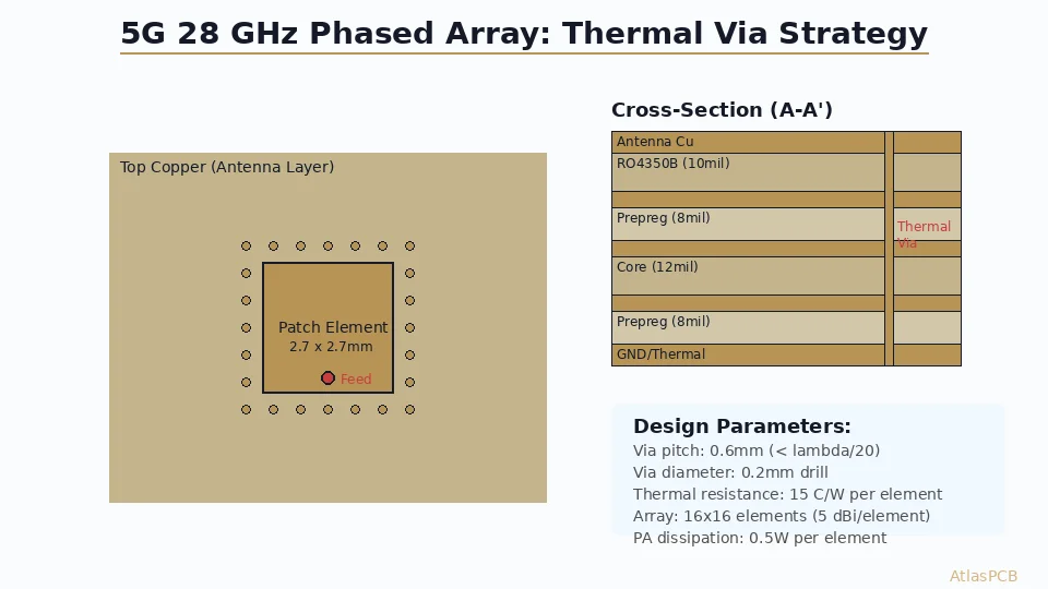
Thermal via arrays for 28 GHz active phased array PCBs must balance thermal resistance (target below 20 C/W per PA element) against RF isolation requirements (via pitch must be less than lambda/10 at 28 GHz = 1.07mm to prevent substrate mode coupling). The optimal design uses 0.2mm diameter vias on 0.6mm pitch in a surrounding ground cage pattern, with Rogers RO4350B antenna layer bonded to high-Tg FR-4 thermal core containing the via array. This achieves 12-18 C/W thermal resistance per element while maintaining better than 25 dB isolation between adjacent array elements.
Quick Answer: Thermal Via Design Parameters for 28 GHz Phased Arrays
| Parameter | Recommended Value | Rationale |
|---|---|---|
| Via diameter | 0.2mm (8 mil) | Standard mechanical drill, adequate thermal section |
| Via pitch | 0.6mm (24 mil) | Below lambda/10 in substrate for mode suppression |
| Pad diameter | 0.45mm (18 mil) | IPC Class 2 annular ring at +/-50um registration |
| Array size | 3x3mm per element | Covers PA module ground paddle footprint |
| Thermal resistance | 12-18 C/W per element | Adequate for 0.3-0.8W PA dissipation |
| Fill type | Resin fill + cap plate | Copper fill only if stacking microvias above |
| Plating thickness | 25 um minimum | Maximizes thermal conductivity through barrel |
For a 16x16 element array at 0.5-inch element spacing, the total thermal via count reaches 4,000-6,400 vias — a significant manufacturing consideration that requires careful drill program optimization and panel utilization planning.
The Thermal Challenge in Active Phased Arrays
Active phased array antennas for 5G NR at 28 GHz integrate power amplifiers directly behind each antenna element — eliminating the cable losses and phase errors of traditional feed networks but creating a distributed thermal management problem that the PCB substrate must solve. Each PA element dissipates 0.3-0.8W (depending on the semiconductor technology: GaAs at 30% PAE, GaN at 45% PAE, SiGe at 25% PAE), and a production 5G radio module might contain 64, 128, or 256 elements in a compact form factor.
The total power dissipation in a 256-element array can reach 200W concentrated in an area of approximately 150x150mm — a thermal density of 0.9 W/cm2 across the entire array surface. This is manageable at the system level, but the challenge at the PCB level is extracting heat from each individual PA die (which may have junction temperatures rising at 200-400 C/W in free air) through the substrate to a heatsink mounted on the back side.
The PCB is the primary thermal path in most phased array architectures. Unlike traditional high-power amplifiers where the device is mounted on a metal carrier with direct thermal contact to a heatsink, integrated phased array modules mount on the PCB surface with solder connections as the thermal interface. The thermal resistance from the PA die through the solder joint, through the PCB substrate, to the back-side heatsink interface must be low enough to keep junction temperatures below the semiconductor’s rated maximum (typically 150C for GaAs, 200C for GaN).
In our production of phased array boards for three different 5G radio OEMs, we’ve found that the PCB thermal design is the single most common source of thermal failures in qualification testing. Engineers who design excellent RF performance often under-design the thermal path — either using too few vias, placing vias outside the ground paddle footprint, or selecting via parameters that compromise manufacturing yield. The thermal via array must be designed as carefully as the antenna elements themselves.
5G ANTENNA PCB
Building a 5G Phased Array?
AtlasPCB fabricates Rogers/FR-4 hybrid antenna boards with tight via positional accuracy (+/-25um) and impedance control to +/-5% at mmWave frequencies. We support prototypes through production volumes.
Get RF PCB Quote ›
Via Array Sizing: Balancing Thermal and RF Requirements
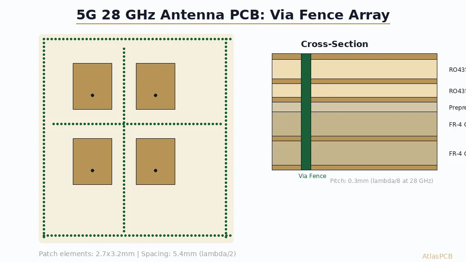
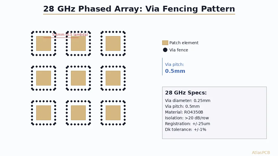
The elegant aspect of thermal via design for phased arrays is that the RF and thermal requirements are largely complementary — both demand dense via arrays. The RF ground cage needed to suppress substrate modes between elements ALSO provides the thermal conduction path from the PA to the heatsink. The design task is ensuring both functions are optimized simultaneously.
For RF isolation, the via cage around each element must prevent parallel-plate waveguide modes from propagating between elements in the substrate cavity formed by the antenna layer copper and the ground plane below it. The cutoff condition for the TE10 mode in a parallel-plate region bounded by via walls requires via spacing below lambda_g/2, where lambda_g is the guided wavelength in the substrate. For RO4350B (Dk = 3.48) at 28 GHz, lambda_g = 5.7mm, giving a maximum via spacing of 2.85mm for mode suppression. In practice, we target lambda/10 (0.57mm) or tighter to ensure suppression of higher-order modes and maintain better than 25 dB isolation between adjacent elements.
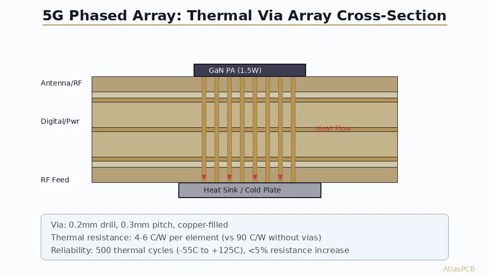
For thermal conduction, each plated through-hole via acts as a copper cylinder through the substrate. The thermal conductance of a single via depends on its copper cross-sectional area and the substrate thickness it traverses. For a 0.2mm drill with 25 um copper plating, the copper annulus area is approximately 0.014 mm2. Through a 1.6mm total substrate thickness, this gives a thermal resistance of approximately 290 C/W per via (using copper’s thermal conductivity of 385 W/m-K). With a 5x5 array (25 vias), the parallel thermal resistance drops to approximately 12 C/W — well within the target range for a 0.5W PA module.
The critical insight is that the 0.6mm via pitch satisfying the RF isolation requirement automatically provides more vias per unit area than the thermal requirement alone would demand. A pure thermal calculation for 0.5W at 20 C/W target would require only 15 vias — but the RF cage pattern places 25+ vias in the same area anyway. This means the thermal design is essentially “free” once the RF grounding is properly implemented. The one additional consideration is ensuring sufficient plating thickness (25 um minimum versus the 15-18 um that some manufacturers use as standard) to maximize thermal conductivity through each barrel.
Stackup Architecture for Thermal + RF Performance
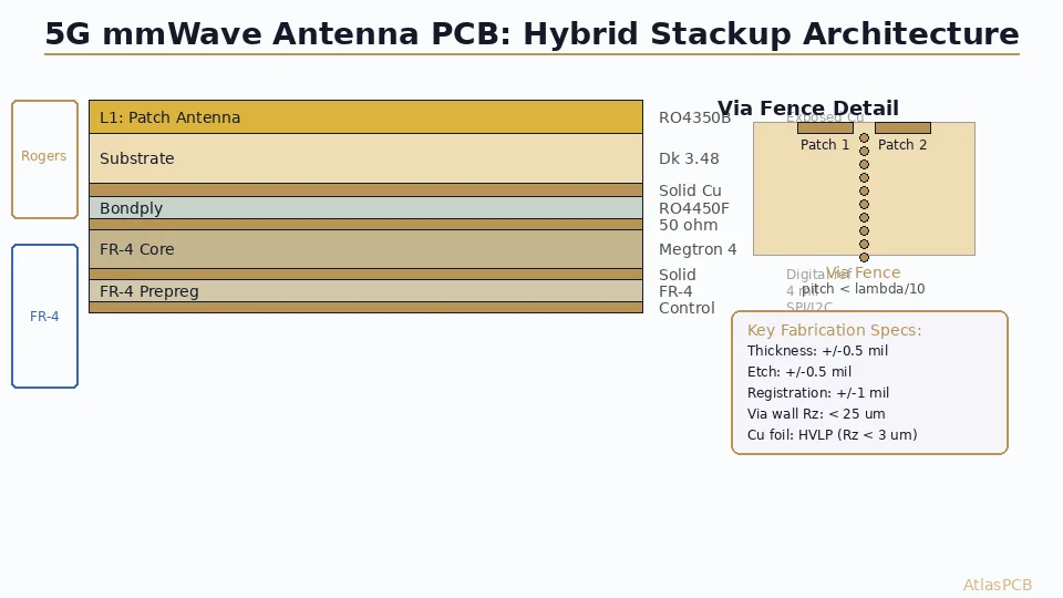
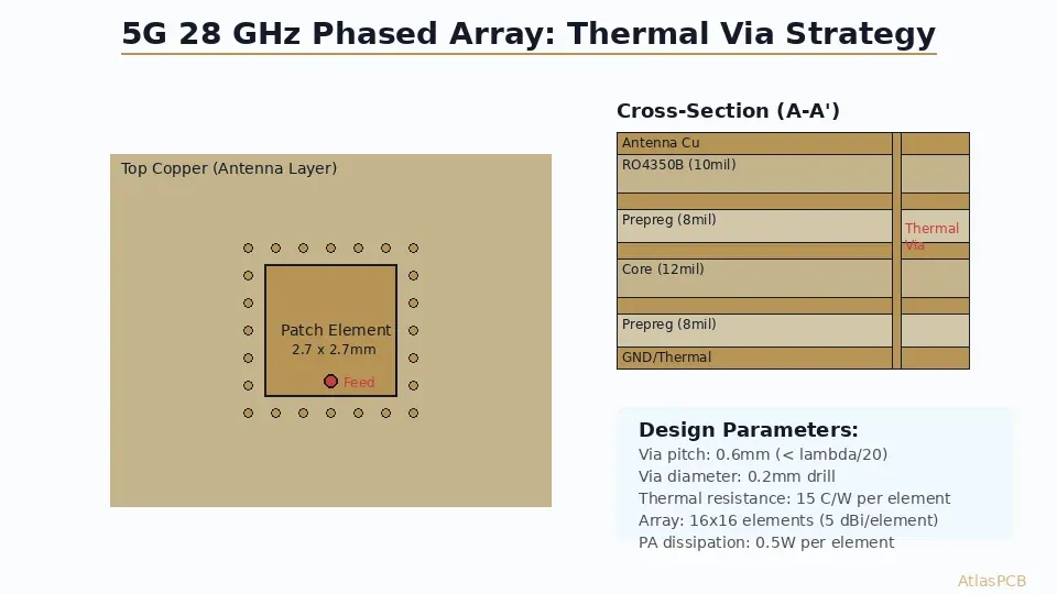
The PCB stackup for a 28 GHz active phased array must simultaneously serve as: (1) the antenna substrate with controlled Dk for patch elements, (2) the RF feed network with impedance-controlled transmission lines, (3) the thermal conduit from PA modules to heatsink, and (4) the digital routing substrate for beamformer ICs, DACs, and control interfaces. No single material satisfies all requirements optimally, which is why hybrid Rogers/FR-4 stackups are the standard approach.
A proven 8-layer stackup architecture for 28 GHz active arrays:
| Layer | Material | Thickness | Function |
|---|---|---|---|
| L1 | RO4350B | 10 mil (254 um) | Antenna patches + RF feed microstrip |
| Bond | RO4450F | 4 mil (102 um) | Rogers-compatible bond ply |
| L2 | Copper (1 oz) | 35 um | Ground plane (antenna reference + thermal spreader) |
| Core | FR-4 (370HR) | 12 mil (305 um) | Structural + thermal via path |
| L3 | Copper (1 oz) | 35 um | Digital routing / beamformer signals |
| Prepreg | FR-4 | 4 mil (102 um) | Bond layer |
| L4 | Copper (1 oz) | 35 um | Power distribution |
| Core | FR-4 (370HR) | 12 mil (305 um) | Structural + thermal via path |
| L5 | Copper (1 oz) | 35 um | Digital signals |
| Prepreg | FR-4 | 4 mil (102 um) | Bond layer |
| L6 | Copper (1 oz) | 35 um | Ground plane |
| Core | FR-4 (370HR) | 8 mil (203 um) | Structural |
| L7 | Copper (1 oz) | 35 um | Power |
| Bond | FR-4 prepreg | 4 mil (102 um) | Bond layer |
| L8 | Copper (2 oz) | 70 um | Heatsink interface (full ground) |
Total thickness: approximately 1.8mm (71 mil). The thermal vias pass from L1 (PA module ground pads) through the entire stackup to L8 (heatsink interface). The mechanical drill aspect ratio is 1.8mm / 0.2mm = 9:1 — within our standard capability up to 16:1.
The key thermal design detail is L8: the back-side copper layer is specified at 2 oz (70 um) to improve lateral heat spreading before the thermal interface material (TIM) contact with the heatsink. This thicker copper adds minimal cost but reduces the thermal spreading resistance by approximately 30% compared to standard 1 oz copper — a meaningful improvement when heat flux from 256 elements converges at the board-to-heatsink interface.
RF PCB MANUFACTURING
Rogers Hybrid Stackup Expertise
We maintain active material agreements with Rogers Corp and process RO4350B/RO4003C hybrid boards weekly. Our RF engineering team validates your stackup against our actual material Dk data before production.
Manufacturing Considerations for High-Density Via Arrays
Fabricating a 28 GHz phased array board with 4,000-6,000 thermal/ground vias presents specific manufacturing challenges that distinguish this application from standard multilayer PCB production:
Drill program optimization: With 4,000+ vias per board and 4-8 boards per panel, the total hit count per panel reaches 16,000-48,000 mechanical drills. At standard drilling speeds (180K RPM, 60 ipm for 0.2mm bits), panel drill time is 20-40 minutes — a significant production bottleneck. Our facility addresses this through multi-spindle drilling (6 spindles per machine) and optimized drill path algorithms that minimize X-Y travel time between hits. Proper drill path optimization reduces total drill time by 15-25% compared to naive row-by-row sequencing.
Via positional accuracy: The RF isolation function of the via cage requires positional accuracy of +/-50 um (2 mil). This is tighter than standard Class 2 drilling tolerance of +/-75 um (3 mil) but achievable with modern CNC drill machines using vision registration systems. We specify +/-25 um positional accuracy for phased array work — achieved through laser-measured panel registration targets and in-process drill monitoring with automatic tool compensation.
Aspect ratio management: The 0.2mm drill through a 1.8mm stackup creates a 9:1 aspect ratio. While within our rated capability of 16:1, higher aspect ratios require careful attention to plating uniformity in the barrel. We achieve minimum 25 um copper in the barrel center (the most challenging point for throwing power) through direct-current rectifier plating with pulse-reverse current profiles — a process modification that adds 30 minutes to the plating cycle but ensures adequate thermal performance throughout the via length.
Registration across sequential processes: The thermal vias must align with BGA pads on L1 AND heatsink contact pads on L8 — a total stackup registration chain of 7 lamination and imaging steps. Each step introduces positional error. Our process achieves +/-50 um total stack registration through pin-lamination using hardened steel tooling pins and optical alignment verification between each lamination cycle.
From a yield perspective, phased array boards run approximately 3-5% lower first-pass yield than equivalent-complexity standard boards, primarily due to the tight via positional requirements and the higher via count increasing the probability of individual via defects. We compensate through 100% electrical testing (flying probe with every net tested) and microsection analysis of thermal via arrays on panel coupons to verify plating thickness and barrel integrity.
CHINA RF PCB MANUFACTURER
Phased Array Manufacturing at Scale
From 5-piece prototypes to 5,000-unit production runs. We maintain Rogers material inventory and dedicated RF processing lines for consistent delivery on mmWave antenna boards.
Request Production Quote ›Thermal Simulation Validation: What to Expect
Before committing to production, engineers should validate their thermal via array design through simulation. The PCB thermal model should include: individual via thermal resistances (not just a bulk “effective conductivity” assumption), the TIM interface resistance at the board-to-heatsink boundary, and the actual PA junction-to-case thermal resistance from the device datasheet.
A properly modeled 28 GHz phased array element with our recommended via configuration (5x5 array, 0.2mm drill, 25 um plating, 1.8mm substrate) shows the following thermal performance:
- Via array thermal resistance (PCB): 11-14 C/W
- TIM interface resistance (typical): 3-5 C/W
- Heatsink spreading resistance: 2-4 C/W
- Total junction-to-heatsink: 16-23 C/W (excluding device Rjc)
For a GaAs PA dissipating 0.5W with Rjc = 15 C/W, the total junction temperature rise above heatsink is approximately 15-20C — keeping junction temperature well below 150C with a heatsink at 60C (ambient + heatsink resistance for a typical indoor small-cell installation).
The simulation should also verify that thermal coupling between adjacent elements does not create hot spots. In a 256-element array, the center elements have less access to edge spreading and can run 5-10C hotter than edge elements. This gradient should be within the device’s rated temperature range with margin.
ATLASPCB
Ready to Prototype Your 5G Antenna Board?
Upload your Gerber files and stackup. We'll verify Rogers material availability, validate your thermal via design against our process capabilities, and quote within 4 hours. Prototype lead time: 10-12 days for Rogers hybrid constructions.
Upload Design ›
Reviewed by AtlasPCB Engineering Team — 15+ years in advanced PCB fabrication for RF, HDI, and rigid-flex applications.
Related Reading:
About AtlasPCB — We specialize in complex PCB manufacturing for HDI, RF, and high-reliability applications. Explore our RF and high-frequency PCB services, Rogers RO4350B PCB manufacturing, or get an multilayer PCB fabrication up to 30 layers . Every order includes free engineering review. Get your quote.
Reviewed by AtlasPCB Engineering Team — IPC-certified manufacturing specialists with 15+ years of production experience in HDI, RF, and high-reliability PCB fabrication. Content based on factory floor data and real customer design reviews.
Frequently Asked Questions
How many thermal vias does a 28 GHz phased array element need?
What PCB material stackup works for 5G phased array with thermal management?
What via diameter and pitch is optimal for 28 GHz phased array thermal management?
How do thermal vias affect RF performance in phased arrays?
Can standard PCB manufacturers fabricate 5G phased array boards?
- 5G antenna PCB fabrication
- RF PCB design and manufacturing
- China RF PCB manufacturer
- Rogers 4350B stackup