· AtlasPCB Engineering · Engineering · 12 min read
5G Antenna PCB Fabrication: Thermal Via Arrays and Power Handling at 28 GHz for Active Phased Arrays
Manufacturing requirements for 5G mmWave active phased array antenna PCBs — covering thermal via array design for GaN PA heat dissipation, Rogers/PTFE material selection for 28 GHz operation, and the fabrication process controls that determine array-level amplitude and phase uniformity.
Quick Answer
Active phased array antenna PCBs for 5G mmWave at 28 GHz require thermal via arrays with 0.3mm pitch and 0.2mm drill beneath each GaN PA die to achieve thermal resistance below 5 C/W, Rogers RO4350B or RO4003C laminate with Dk uniformity better than +/-2% across the array aperture for consistent element-to-element phase, and manufacturing tolerance on via position within +/-25 microns to prevent pattern distortion from asymmetric parasitic coupling.
Quick Answer: Critical PCB Specs for 28 GHz Phased Arrays
| Parameter | Requirement | Why It Matters |
|---|---|---|
| Laminate | Rogers RO4350B or RO4003C | Dk uniformity and low Df at 28 GHz |
| Dk uniformity | Better than +/-2% across panel | Element-to-element phase consistency |
| Thermal via pitch | 0.3mm center-to-center | Thermal resistance < 5 C/W per element |
| Thermal via drill | 0.2mm (mechanical) or 0.15mm (laser) | Maximizes copper thermal path area |
| Via position tolerance | +/-25 microns | Prevents parasitic coupling asymmetry |
| Etch tolerance (patch) | +/-0.5 mil (12.5 um) | Maintains resonant frequency within spec |
| Layer registration | +/-25 microns | Slot/aperture alignment accuracy |
| Surface finish | ENIG (2-5 uinch Au) | Consistent conductor loss at mmWave |
| Board flatness | < 0.5% warp | Required for proper heat sink contact |
These specifications are achievable in volume production with the right manufacturer and process controls, but they collectively represent a significantly tighter process window than standard multilayer PCB fabrication.
The Thermal Problem in Active Phased Arrays
Active phased arrays fundamentally changed the thermal management challenge in antenna PCB design. Traditional passive arrays and even semi-active systems concentrated heat at a few discrete RF modules. Modern 5G mmWave active arrays distribute amplification across every element — 64, 128, or 256 individual power amplifiers, each dissipating 0.5-2W in a die area smaller than 10 mm2.
The total thermal load on a 128-element array operating at full power reaches 100-250W, and this heat must be removed through the PCB substrate because the component-side surface is occupied by antenna elements that cannot be blocked by heatsink hardware. The only practical thermal path is downward through the PCB to a cold plate or heat sink mounted on the back side.
PCB materials are poor thermal conductors. FR-4 has thermal conductivity of approximately 0.3 W/m-K through-thickness, and even Rogers RO4350B is only marginally better at 0.69 W/m-K. For a 1.6mm board thickness with a 3x3mm thermal pad, the thermal resistance through solid dielectric would be approximately 90 C/W — completely inadequate for a PA dissipating 1.5W (that would create a 135C temperature rise above the heatsink temperature).
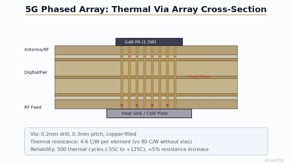
Thermal via arrays solve this by replacing the dielectric thermal path with copper-filled columns. Copper’s thermal conductivity is 400 W/m-K — nearly 600x better than Rogers laminate. A properly designed thermal via array can reduce the PCB thermal resistance to 3-6 C/W, making conduction cooling through the substrate practical for power levels up to 2W per element.
5G ANTENNA PCB SPECIALISTS
Thermal Via Arrays for mmWave Active Arrays
0.15mm laser vias, 0.25mm pitch arrays, copper-filled for thermal conductivity. Rogers RO4350B hybrid stackups with verified Dk uniformity across the panel.
Get Phased Array PCB Quote ›
Thermal Via Array Design: Geometry That Actually Works
The thermal via array design involves balancing three competing constraints: thermal resistance (wants maximum copper area), electrical isolation (vias must not couple to adjacent RF traces), and mechanical reliability (via density cannot exceed the stress limits of the laminate during thermal cycling).
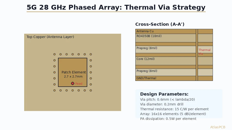
Via diameter and pitch: The standard approach uses 0.2mm finished hole diameter on 0.3mm pitch in a rectangular array beneath the PA thermal pad. For a typical 3x3mm thermal pad, this creates a 10x10 via array (100 vias per element). Each via contributes approximately 0.05 C/W thermal resistance in parallel, producing a combined array thermal resistance of approximately 5 C/W for a 1.6mm board. Increasing to 0.25mm pitch with 0.15mm laser vias (possible with HDI processing) adds 60% more vias per unit area, reducing thermal resistance to approximately 3 C/W.
Copper fill requirement: For thermal vias to achieve their theoretical conductivity, they must be copper-filled — not merely plated through-holes. A standard plated via with 25-micron wall plating has a hollow center that dramatically reduces its effective thermal conductivity (approximately 30% of a solid copper column). Copper-filled vias with electroplated fill achieve 85-95% of solid copper thermal performance. In our process, we use pulse-reverse plating to achieve void-free copper fill in 0.2mm holes, verified by microsection analysis on thermal coupon samples.
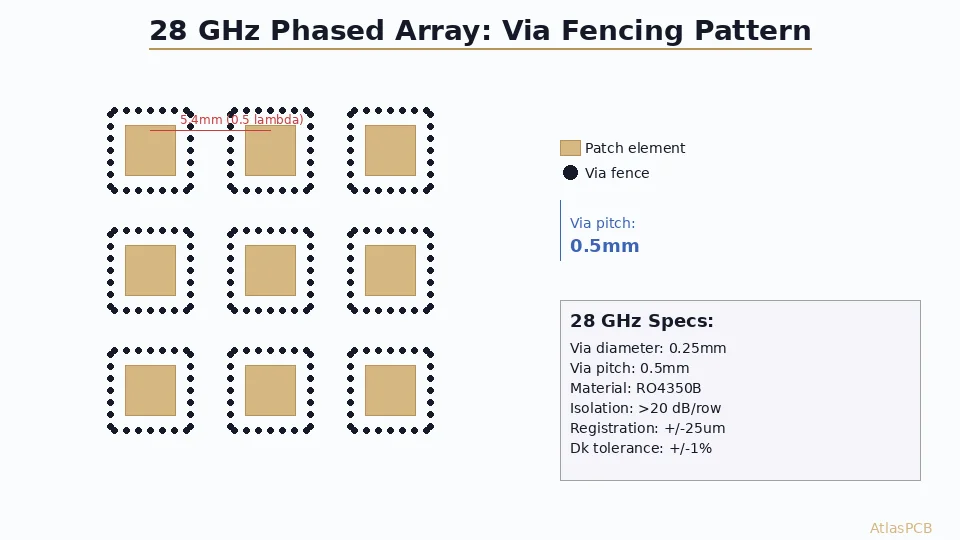
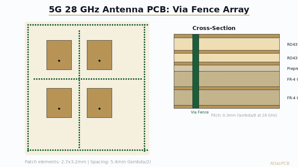
Via-to-trace isolation: The thermal via array must not parasitically couple to the RF feed lines or adjacent antenna elements. At 28 GHz, vias act as waveguide elements and can support resonant modes if their spacing exceeds approximately lambda/4 (2.7mm in FR-4 or 2.5mm in Rogers). Fortunately, the tight 0.3mm pitch keeps the via array well below resonant spacing. However, the outer ring of vias in the array must maintain clearance to any RF traces of at least 3x the substrate height to prevent impedance perturbation.
Reliability under thermal cycling: Dense via arrays concentrate thermo-mechanical stress at the via-to-pad interfaces during temperature excursions. For 5G infrastructure operating -40C to +85C with power cycling, we design thermal via arrays with minimum 0.1mm annular ring (pad diameter at least 0.4mm for 0.2mm drill) and specify IPC Class 3 barrel plating thickness (minimum 25 microns). Reliability qualification includes 500 thermal cycles per IPC-6012 with less than 5% resistance increase on daisy-chain test structures.
Material Selection: Dk Uniformity Across the Array Aperture
For a phased array to produce a well-formed beam with predictable sidelobe levels, each antenna element must radiate with correct amplitude and phase relative to its neighbors. The PCB contributes to element-to-element phase variation through dielectric constant non-uniformity across the panel area.
A 128-element array at half-wavelength spacing covers approximately 70x70mm at 28 GHz. Across this area, the Rogers laminate must maintain Dk uniformity sufficient to keep phase error below the array’s error budget — typically 5 degrees RMS for -20 dB sidelobes.
The relationship between Dk variation and phase error is approximately: phase_error (degrees) = 360 * (feed_length / wavelength) * (delta_Dk / (2 * sqrt(Dk))). For a 20mm feed line at 28 GHz on RO4350B, a Dk variation of +/-2% (3.48 +/- 0.07) produces approximately 4 degrees of phase error per element. This is at the edge of acceptable for most arrays.
In our production, we verify Dk uniformity using two methods. First, we procure Rogers laminate from the same production lot for the entire array panel run, ensuring batch-to-batch Dk variation doesn’t contribute to element variation within a single array. Second, we measure impedance on test coupons placed at four quadrants of the production panel — if any coupon deviates more than 1.5% from the average, the panel is flagged for review before array population.
This level of material control is not standard practice at most PCB manufacturers. It requires incoming material verification capability, lot tracking discipline, and a willingness to reject panels that pass general impedance tolerance but fail array-specific uniformity requirements. This is where a China RF PCB manufacturer with phased array experience differentiates from a general-purpose fab.
ARRAY-GRADE MATERIAL CONTROL
Panel-Level Dk Uniformity Verification
Single-lot material procurement, quad-position impedance monitoring, and reject criteria tighter than general-purpose tolerance — because array performance demands it.
RF PCB Capabilities ›Fabrication Process Controls for Array-Grade PCBs
Beyond material selection and via array design, several fabrication process steps require tighter control for phased array antenna PCBs than for general RF boards:
Etch uniformity for patch elements: Each antenna patch in the array must be dimensionally identical within tolerance. At 28 GHz, the resonant frequency of a patch shifts approximately 80-120 MHz per mil (25 microns) of dimensional change. For the array to operate within a 500 MHz band without individual element frequency correction, patch dimensions must be controlled to +/-0.5 mil. This requires etch process uniformity better than standard production — achieved through fresh chemistry monitoring, spray pressure balancing across the panel width, and etching Rogers panels in dedicated runs (not mixed with FR-4 which has different etch rates).
Registration for aperture-coupled designs: Multilayer array antennas often use aperture coupling (a slot in the ground plane feeds energy from a buried microstrip to a radiating patch above). The slot position relative to the patch determines coupling efficiency and operating bandwidth. Registration error between the slot layer and patch layer must be held to +/-25 microns — achievable with optical alignment systems but requiring explicit specification and verification on the first article panel.
Surface finish uniformity: ENIG is the standard finish for mmWave arrays because it provides consistent conductor surface across all exposed copper. Gold thickness variation directly affects conductor loss — thicker gold on some pads creates insertion loss non-uniformity across the feed network. We specify ENIG thickness at 3-5 microinches gold with panel-to-panel variation less than 1 microinch, achieved through SPC monitoring of the electroless gold bath.
Board flatness for heatsink bonding: After all processing, the PCB must be flat enough for uniform thermal interface material (TIM) contact with the heatsink. Phased array PCBs with dense thermal via arrays are susceptible to local warpage because the via fields create regions with different CTE than the surrounding dielectric. Our process includes post-bake flattening at 150C with controlled cooling, achieving flatness better than 0.5% of the diagonal dimension (typically less than 0.5mm bow over a 100mm panel).
Production Example: 64-Element 28 GHz Array Module
To illustrate how these requirements come together, here is the specification summary for a 64-element active array PCB we recently produced for a 5G small cell manufacturer:
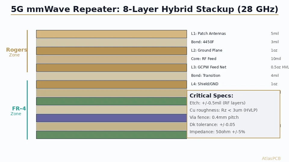
Stackup: 8-layer hybrid — Rogers RO4350B (20 mil) on L1 (antenna/patch), FR-4 core for inner layers (power, ground, digital control), Rogers RO4350B (10 mil) on L8 (RF feed network). Total thickness 1.8mm.
Thermal vias: 0.2mm drill, 0.3mm pitch, 8x8 array (64 vias) per PA element. Copper-filled, planarized. Total 4,096 thermal vias across the panel.
RF performance achieved: Impedance uniformity across the 64-element aperture: 50 ohms +/-3.5% (better than the +/-5% specification). Dk variation measured across the panel: +/-1.2%. Feed network insertion loss: 1.8 dB total (exceeding the 2.5 dB budget).
Thermal result: Measured thermal resistance from PA junction to heatsink contact: 4.2 C/W per element. At 1.5W dissipation per element and heatsink temperature of 55C, PA junction temperature reached 61.3C — well within the 150C absolute maximum.
Yield: First-article pass rate: 95% (3 of 64 elements marginally out of phase spec). Production yield after process optimization: 98.5% at element level.
This project demonstrated that array-grade RF PCB fabrication is achievable in volume production from a qualified China RF PCB manufacturer with appropriate process controls and material management — at significantly lower cost than domestic (US/EU) RF fab houses while meeting identical electrical specifications.
PHASED ARRAY PRODUCTION
From 28 GHz Prototype to Volume Production
We have produced 5G mmWave phased array PCBs for small cells, CPE modules, and radar systems. Thermal via arrays, Rogers hybrid stackups, array-grade process control.
Discuss Your Array Design ›Selecting a Manufacturer for 5G Antenna PCB Fabrication
Phased array antenna PCBs sit at the intersection of RF material expertise, HDI via processing, and thermal management — a combination that few manufacturers handle routinely. When evaluating potential suppliers, the discriminating questions:
Do they have Rogers hybrid stackup experience? Ask for cross-section photos of previous Rogers/FR-4 hybrid builds showing the bondply interface quality.
Can they copper-fill thermal vias at 0.2-0.3mm pitch? Request microsection images showing void-free fill at these geometries. Many manufacturers claim copper fill but achieve only 70-80% fill ratio at tight pitches.
What is their via position accuracy? The +/-25 micron requirement for array-grade work means optical alignment, not pin registration. Verify they measure and report registration data.
Do they characterize Dk across the panel? Most manufacturers measure impedance at one or two coupon positions. Array work requires four-quadrant verification or full TDR scanning.
Have they produced antenna PCBs with measured RF performance data? A manufacturer who has shipped arrays with documented radiation pattern and return loss data understands the requirements at a system level, not just board-level specifications.
The 5G infrastructure buildout has created a capable tier of China RF PCB manufacturers who routinely produce phased array boards for both domestic 5G deployment and export customers. Material costs are identical (Rogers pricing is global), but fabrication costs run 30-50% lower than US/EU equivalents for the same specification level. The key is finding manufacturers with genuine array fabrication experience rather than general-purpose shops attempting their first mmWave antenna board.
ATLASPCB
China RF PCB Manufacturer — 5G Antenna Arrays in Production
Rogers RO4350B/4003C in stock. Copper-filled thermal vias at 0.25mm pitch. Array-grade Dk uniformity verification. From prototype validation to volume production.
Get 5G Array PCB Quote ›
Reviewed by AtlasPCB Engineering Team — 15+ years in advanced PCB fabrication for RF, HDI, and rigid-flex applications.
Related Reading:
About AtlasPCB — We specialize in complex PCB manufacturing for HDI, RF, and high-reliability applications. Explore our RF and high-frequency PCB services, Rogers RO4350B PCB manufacturing, or get an multilayer PCB fabrication up to 30 layers . Every order includes free engineering review. Get your quote.
Reviewed by AtlasPCB Engineering Team — IPC-certified manufacturing specialists with 15+ years of production experience in HDI, RF, and high-reliability PCB fabrication. Content based on factory floor data and real customer design reviews.
Frequently Asked Questions
Why do 5G phased array antenna PCBs need thermal via arrays?
What via array pitch is needed for adequate thermal performance?
How does via position accuracy affect phased array performance?
Which PCB material is best for 28 GHz antenna arrays?
What manufacturing tolerances matter most for phased array PCBs?
- 5G antenna PCB fabrication
- China RF PCB manufacturer
- Rogers 4350B stackup
- RF PCB design and manufacturing
- thermal management