· Industry News · 6 min read
IMS 2026 Wrap-Up: RF PCB Technology Trends from the IEEE Microwave Symposium in Boston
Key RF and microwave PCB technology developments from IEEE IMS 2026 (June 8-13, Boston). Coverage of substrate-integrated waveguide advances, mmWave packaging trends, GaN-on-PCB integration, and what these developments mean for high-frequency board fabrication in 2026-2027.
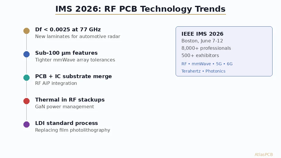
Key Takeaways for PCB Engineers
IEEE IMS 2026, which concluded yesterday (June 13) in Boston, showcased several developments directly relevant to PCB fabrication and ordering decisions. Here’s what matters for engineers specifying high-frequency boards in the near term.
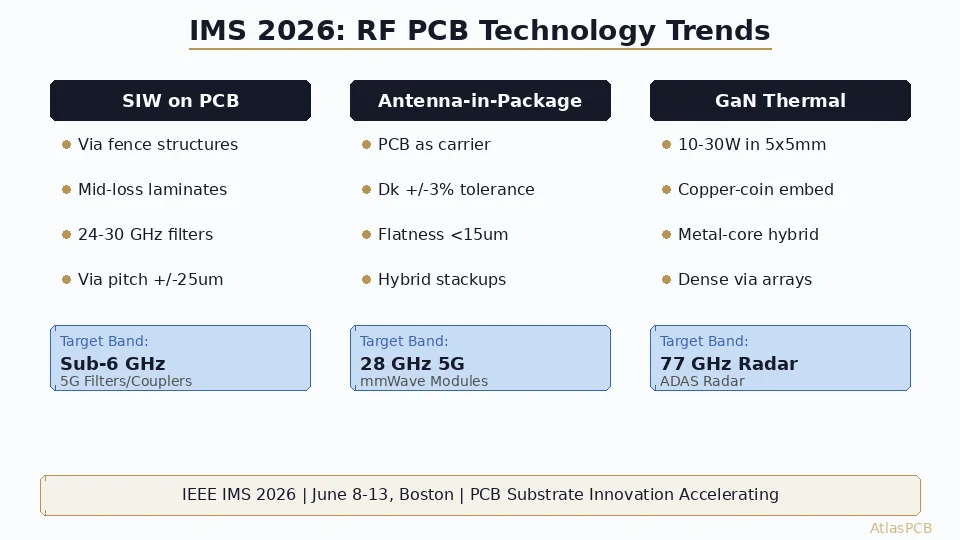
SIW Filters Moving from Lab to Production PCBs
Substrate-integrated waveguide (SIW) technology — where via fences in PCB laminate create waveguide-like structures — was a dominant topic across technical sessions and industry exhibits.
What changed in 2026: Multiple exhibitors demonstrated SIW bandpass filters and couplers fabricated on mid-loss laminates (Megtron 6 class, Dk ~3.4, Df ~0.002) rather than requiring pure PTFE substrates. This represents a significant cost reduction for 24-30 GHz applications.
PCB fabrication implications:
- Via pitch tolerance becomes critical: SIW performance depends on via-to-via spacing accuracy (typically +/-25um required)
- Via diameter uniformity matters more than individual via size
- Standard 0.2mm mechanically drilled vias work for sub-6 GHz SIW; 28 GHz and above require 0.1-0.15mm laser vias
- Copper surface roughness (HVLP foil, Rz < 2um) is specified to reduce conductor loss in the waveguide walls
For designs using SIW structures, ensure your fabricator can hold via pitch tolerance across the full panel. This is a registration and drill accuracy specification, not just a drill size spec.
For background on SIW design principles, see our technical guide on substrate-integrated waveguide PCB design for mmWave applications.
RF PCB FABRICATION
SIW-Capable PCB Manufacturing
Via pitch accuracy to +/-25um, laser drilling for mmWave SIW, and HVLP copper on Megtron 6 and Rogers laminates. Production-proven for 5G and radar applications.
Request RF PCB Quote ›Antenna-in-Package: PCB as the “Last Mile” Interconnect
Several papers and demos focused on antenna-in-package (AiP) modules for 60 GHz and 77-81 GHz applications. While the antenna itself sits within the IC package, the PCB carrying the module must meet specific requirements:
PCB substrate requirements for AiP modules:
- Controlled Dk tolerance: +/-3% across the board (tighter than standard +/-5%)
- Surface flatness: < 15um deviation over component footprint area
- Landing pad coplanarity for package attach: < 50um
- Thermal via arrays under module for heat extraction (GaN PAs dissipating 5-15W)
- Hybrid stackup common: Rogers/PTFE top layers + standard FR-4 core for cost optimization
The opportunity for PCB fabricators: As AiP replaces discrete antenna arrays, the PCB transitions from carrying individual antenna patches to providing mechanical/thermal support for integrated modules. This actually simplifies the RF layers but tightens flatness and thermal requirements.
GaN Power Amplifier Integration: Thermal PCB Challenges
GaN-based power amplifiers for 5G base stations and radar were extensively demonstrated. The key PCB challenge: removing 10-30W of heat from a 5x5mm package through the board.
Thermal solutions discussed at IMS 2026:
Copper-coin embedding: Machined copper slugs press-fit into PCB cavities directly under the GaN package. Thermal resistance through-board drops from ~40 C/W (FR-4) to ~2-5 C/W.
Metal-core hybrid stackups: Aluminum or copper-core substrates for the PA section, laminated with standard FR-4 for digital control circuitry. Requires multi-material bonding expertise.
Thermal via arrays with conductive fill: Dense via arrays (0.3mm pitch, 0.15mm diameter) with copper epoxy fill under the PA footprint. More compatible with standard PCB processes than coin embedding.
AtlasPCB’s aluminum and copper metal-core PCB capabilities directly address these thermal management requirements. See our aluminum PCB thermal design guide for relevant specifications.
HIGH-FREQUENCY CAPABILITIES
Rogers, PTFE, and Hybrid RF Stackups
We fabricate hybrid stackups combining Rogers 4350B/4003C RF layers with standard FR-4 cores. Metal-core options for GaN thermal management. Impedance-controlled to +/-5%.
Upload RF Design ›New Low-Loss Laminate Announcements
Laminate suppliers at IMS 2026 introduced next-generation products targeting the 77-81 GHz automotive radar band:
- Dk stability vs temperature: New formulations claim +/-2% Dk variation from -40C to +125C (automotive operating range), compared to +/-5% for current Rogers 4350B
- Ultra-low profile copper: Rz < 1.0um foils becoming available for 77 GHz loss reduction (previously only available at lab scale)
- Halogen-free PTFE alternatives: Meeting both RF performance and automotive environmental compliance (IEC 61249-2-21)
These materials will begin appearing in production PCB supply chains in late 2026 to early 2027. For current 77 GHz projects, Rogers RO3003 and RO4835 remain the established choices.
Impact on PCB Ordering: What to Do Now
If you’re designing RF/microwave boards in the next 6 months, IMS 2026 developments suggest:
For 5G/28 GHz designs: Consider SIW on Megtron 6 as a cost-effective alternative to pure PTFE for filter/coupler structures. Specify via pitch tolerance explicitly in your fab drawing.
For 77 GHz automotive radar: Current material set (RO3003, RO4835) remains appropriate. New ultra-low-roughness options coming but not production-ready until Q1 2027.
For GaN PA boards: Specify thermal via arrays with conductive fill, or inquire about copper-coin embedding capability. Metal-core hybrid is viable for prototype and low-volume.
For AiP carrier boards: Tighten flatness and Dk tolerance specs beyond standard multilayer. Discuss requirements with your fabricator during design phase, not at quoting.
ATLASPCB
RF and Microwave PCB Fabrication — From Prototype to Production
Rogers, PTFE, Megtron, and hybrid stackups. Impedance-controlled multilayer boards for 5G, radar, and satellite applications. Discuss your RF design requirements with our engineering team.
Get RF PCB Quote ›Related Reading:
About AtlasPCB — We specialize in complex PCB manufacturing for HDI, RF, and high-reliability applications. Explore our RF and high-frequency PCB services . Every order includes free engineering review. Get your quote.
Reviewed by AtlasPCB Engineering Team — IPC-certified manufacturing specialists with 15+ years of production experience in HDI, RF, and high-reliability PCB fabrication. Content based on factory floor data and real customer design reviews.
- ims-2026
- rf-pcb
- microwave
- 5g-mmwave