· AtlasPCB Engineering · News · 9 min read
800V EV Architectures Drive New PCB Thermal and Insulation Design Requirements
The automotive industry's rapid adoption of 800V electrical architectures for EVs is creating demanding new requirements for PCB designers: higher creepage and clearance distances, reinforced insulation materials, heavy copper for high-current paths, and advanced thermal management for SiC power electronics.
800V EV Architectures Drive New PCB Thermal and Insulation Design Requirements
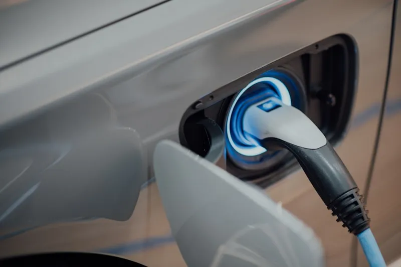
The electric vehicle industry is in the middle of its most significant power architecture transition since the original move from 12V lead-acid to high-voltage battery systems. The shift from 400V to 800V electrical architectures — driven by the need for faster charging, reduced cable weight, and improved inverter efficiency — is now reaching critical mass in the global EV market.
In 2026, 800V is no longer a premium-exclusive technology. While the Porsche Taycan (2019) pioneered the architecture and the Hyundai Ioniq 5/6 and Kia EV6 brought it to the mainstream, the technology has now spread to volume manufacturers including BYD (Han EV, Seal), Xiaomi (SU7), NIO (ET7, ES7), Xpeng (G9), and Lucid (Air). Industry analysts estimate that over 40% of new EV platforms launching in 2026–2028 will use 800V architecture, up from approximately 15% in 2024.
For PCB designers and manufacturers, this transition creates a cascade of new requirements that touch every aspect of board design: insulation distances, material selection, copper weight, thermal management, and reliability qualification. Understanding these requirements is essential for anyone supplying PCBs to the automotive EV supply chain.
Why 800V: The Engineering Rationale
The move to 800V is fundamentally about physics and economics:
Faster charging. Charging power equals voltage × current. At 400V, a 350kW DC fast charger delivers approximately 875A — requiring massive cables, connectors, and cooling systems. At 800V, the same 350kW requires only ~438A, enabling thinner cables, smaller connectors, and lighter cooling hardware. The 800V architecture enables charging rates up to 800kW (theoretical maximum with current battery chemistry), translating to practical charging times of 10–15 minutes for 10–80% state of charge.
Reduced weight and cost. Halving the current for the same power means conductors (wiring harnesses, busbars, PCB traces) can be smaller in cross-section. For a typical EV wiring harness, moving from 400V to 800V saves approximately 15–20kg of copper — significant in a vehicle where every kilogram affects range.
Improved inverter efficiency. SiC (silicon carbide) MOSFETs, which are the enabling device technology for 800V systems, have lower conduction and switching losses than silicon IGBTs used in 400V systems. This translates to 2–5% improvement in drive cycle efficiency, which directly extends vehicle range.
PCB Design Impact: Insulation and Creepage
The most immediate and often underestimated impact of doubling battery voltage is the requirement for increased electrical insulation on all PCBs within the high-voltage domain.
IPC-2221B Creepage and Clearance Requirements
IPC-2221B defines minimum conductor spacing based on working voltage, pollution degree (environmental contamination level), and insulation type. For automotive applications:
| Parameter | 400V System | 800V System | Change |
|---|---|---|---|
| Working voltage | 400V DC | 800V DC | 2× |
| Clearance (through air) at PD2 | 3.2mm | 6.4mm | 2× |
| Creepage (along surface) at PD2, Material Group II | 4.0mm | 8.0mm | 2× |
| Reinforced insulation clearance | 6.4mm | 12.8mm | 2× |
| Reinforced insulation creepage | 8.0mm | 16.0mm | 2× |
These distances are minimum values — most automotive OEMs impose additional margins of 20–50% above IPC minimums in their own specifications. For detailed guidance on managing high-voltage spacing, see our [high-voltage PCB design guide]/blog/high-voltage-pcb-design/).
Design Implications
The doubled insulation distances have profound effects on PCB layout:
- Board area increases. For a gate driver or battery management system (BMS) PCB, the increased creepage requirements can add 20–35% to the board area compared to a 400V equivalent design. This is not trivial in automotive applications where module size is tightly constrained.
- Routing slots and cutouts. Designers frequently use milled slots in the PCB to increase creepage distance without increasing board size. A 1mm-wide slot provides approximately 2× the creepage benefit of the same distance on a flat surface, because contaminants must traverse the slot walls.
- Isolation barrier design. Where the PCB provides the primary isolation between high-voltage and low-voltage domains (e.g., in isolated gate drivers), reinforced insulation requirements apply. This may necessitate dedicated isolation zones on the PCB with no copper, no vias, and no components within the clearance zone.
- High-voltage connectors. PCB footprint design for high-voltage connectors must account for both pin-to-pin spacing and pin-to-ground-plane clearance, often requiring localized ground plane relief.
Material Requirements: Beyond Standard FR-4
Standard FR-4 PCB laminates, while adequate for many automotive applications at 400V, face limitations at 800V:
Comparative Tracking Index (CTI)
CTI measures a material’s resistance to electrical tracking — the formation of conductive paths along the surface due to contamination and voltage stress. IPC-2221B uses CTI to determine required creepage distances:
| Material Group | CTI Range | Creepage Impact |
|---|---|---|
| Group I | ≥600V | Shortest creepage allowed |
| Group II | 400–599V | Standard creepage |
| Group IIIa | 175–399V | Increased creepage (1.5×) |
| Group IIIb | 100–174V | Maximum creepage (2×) |
Standard FR-4 typically has a CTI of 175–250V (Group IIIa), which forces 50% longer creepage distances. High-CTI FR-4 variants (IS410, IT180A) achieve CTI ≥400V (Group II), allowing standard creepage distances and saving precious board area.
For critical applications, our [PCB material selection guide]/blog/pcb-material-selection-guide/) provides detailed comparisons of automotive-grade laminates.
Flame Rating and Thermal Properties
All 800V EV PCBs must meet:
- UL 94 V-0 flame rating (self-extinguishing within 10 seconds)
- Glass transition temperature (Tg) ≥170°C for under-hood and inverter-adjacent locations
- Decomposition temperature (Td) ≥340°C to withstand lead-free soldering and thermal excursions
- Moisture absorption <0.15% to maintain insulation integrity in humid environments
Ceramic-filled laminates offer an attractive combination of high CTI (>600V), low CTE for reliability, and improved thermal conductivity (0.8–1.2 W/m·K vs. 0.3 W/m·K for standard FR-4), though at a significant cost premium.
Heavy Copper for High-Current Paths
800V systems still carry substantial currents — a 200kW inverter at 800V draws approximately 250A at full power. The PCB traces carrying these currents must be designed with appropriate copper weight and thermal considerations.
Copper Weight Selection
| Current Rating | Minimum Copper Weight | Typical Trace Width (40°C rise) |
|---|---|---|
| 10–25A | 2oz (70μm) | 5–15mm |
| 25–50A | 3oz (105μm) | 8–20mm |
| 50–100A | 4oz (140μm) | 12–30mm |
| 100–200A | 6oz (210μm) | 15–40mm |
| >200A | Busbar/copper inlay | N/A |
For detailed heavy copper design guidance, see our [heavy copper PCB guide]/blog/heavy-copper-pcb/).
Copper Inlay and Coin Technology
For the highest current paths (>200A), embedded copper coins or busbars provide a superior alternative to extremely wide heavy-copper traces:
- Copper coins (1–3mm thick press-fit copper slugs) inserted into the PCB laminate provide thermal and electrical paths with resistance 10–100× lower than even 6oz copper traces
- Embedded busbars laminated between PCB layers create defined high-current paths without consuming surface area
- Both technologies require specialized PCB fabrication capabilities and careful design of the transition between the inlay and standard copper layers
Thermal Management: SiC Gate Driver Challenges
The transition to SiC MOSFETs in 800V inverters creates unique thermal challenges for the gate driver PCB — the board that directly controls the power switches.
Why SiC Changes the Thermal Game
SiC MOSFETs switch at 20–50 kHz compared to 5–10 kHz for silicon IGBTs. Higher switching frequency reduces filter component size and improves current waveform quality, but concentrates more switching losses in a smaller die area. The gate driver PCB must:
- Dissipate 5–15W per driver channel from driver ICs and associated power components
- Operate reliably at ambient temperatures of 105–125°C (inverter internal temperature)
- Maintain isolation integrity between the high-voltage gate drive domain and the low-voltage control domain at temperatures up to 150°C
- Minimize parasitic inductance in the gate drive loop (target: <5nH), which affects switching transients and EMI
Thermal Via Design for Gate Drivers
Thermal via arrays are the primary mechanism for conducting heat from top-side thermal pads to bottom-side heatsinks. For 800V gate driver applications, our [thermal via design guide]/blog/pcb-thermal-via-design/) recommends:
- Via diameter: 0.3mm (finished hole), plated shut or filled with conductive epoxy
- Via pitch: 0.6mm center-to-center (achievable with standard drilling)
- Array size: Matched to the thermal pad footprint of the driver IC
- Fill requirement: Conductive epoxy fill (thermal conductivity ~3 W/m·K) or copper-filled (>300 W/m·K for premium applications)
- Thermal resistance: A properly designed via array can achieve <5°C/W from pad to heatsink, compared to 15–25°C/W for bare vias with air-fill
Board-Level Thermal Conductivity
Beyond via arrays, the PCB itself contributes to thermal spreading. Options include:
- Heavy copper inner layers (3–6oz) acting as thermal spreaders
- Metal-core PCB (MCPCB) substrates for single-layer gate driver designs
- Ceramic-filled prepreg with thermal conductivity of 0.8–1.2 W/m·K
- Direct bonded copper (DBC) substrates for the highest-performance applications, though these blur the line between PCB and power module substrate
Automotive Qualification Requirements
PCBs for 800V EV applications must pass rigorous qualification testing beyond standard IPC acceptance criteria:
Reliability Standards
- AEC-Q100 qualification for automotive-grade electronic components
- IATF 16949 quality management system certification for the PCB manufacturer
- Thermal cycling: -40°C to +125°C, 1,000–3,000 cycles minimum (per AEC-Q100 Grade 1)
- Humidity bias: 85°C/85% RH with voltage bias for 1,000 hours
- Vibration: Random vibration per ISO 16750-3 for the duration of vehicle lifetime (15 years/300,000 km)
- Partial discharge testing: Mandatory for reinforced insulation designs, verifying no partial discharge activity below 1.5× working voltage
Meeting [automotive PCB requirements]/blog/automotive-pcb-requirements/) demands close collaboration between PCB designers and qualified manufacturers who maintain automotive production lines and process controls.
Production Traceability
800V EV PCBs require full traceability:
- Lot-level material traceability (laminate, prepreg, copper foil, solder mask)
- Process parameter recording for each production lot
- Electrical test data retention (minimum 15 years per automotive OEM requirements)
- Unique board serialization for safety-critical applications (ASIL C/D per ISO 26262)
Market Opportunity: EV PCB Growth
The EV PCB market represents one of the fastest-growing segments in the industry:
- Global EV PCB market (2025): approximately $8.2 billion
- Projected (2028): approximately $14.5 billion — a CAGR of 25%+
- 800V-specific PCB demand is growing even faster at 35%+ CAGR as the architecture becomes mainstream
- Average PCB content per EV: $180–$350, compared to $50–$80 for ICE vehicles — a 3–4× premium
- Key growth segments: Inverter gate drivers, BMS boards, on-board chargers (OBC), DC-DC converters, and thermal management control boards
For PCB manufacturers with automotive-grade multilayer capabilities, the 800V EV transition represents a significant market opportunity.
What PCB Designers Should Do Now
Audit creepage and clearance distances. If your existing 400V designs are being adapted for 800V, every insulation distance must be re-evaluated. Use IPC-2221B tables with the correct pollution degree and material group.
Specify high-CTI materials. Request Material Group II (CTI ≥400V) laminates from your fabricator to minimize the board area penalty of increased creepage distances.
Plan for heavy copper. If your design carries >25A, work with your fabricator to determine the optimal copper weight and trace width combination for your thermal and current requirements.
Design thermal via arrays early. Thermal management cannot be an afterthought in 800V designs. Define thermal via arrays in the schematic phase, not during layout.
Engage qualified automotive manufacturers. Not all PCB fabricators can produce 800V automotive boards. Verify IATF 16949 certification, heavy copper capability, and high-voltage testing infrastructure.
What This Means for Your Next Project
Whether you’re designing 800V inverter gate drivers, battery management systems, or on-board charger units, Atlas PCB’s engineering team stays ahead of industry developments to deliver optimized solutions. Contact us to discuss how these developments affect your PCB requirements.
About AtlasPCB — We specialize in complex PCB manufacturing for HDI, RF, and high-reliability applications. Explore our aluminum and metal-core PCB services . Every order includes free engineering review. Get your quote.
Reviewed by AtlasPCB Engineering Team — IPC-certified manufacturing specialists with 15+ years of production experience in HDI, RF, and high-reliability PCB fabrication. Content based on factory floor data and real customer design reviews.
- news
- ev
- automotive
- thermal-management
- high-voltage