· AtlasPCB Engineering · Industry News · 6 min read
Citi Raises AI-PCB Market Forecast to RMB 562 Billion by 2028: Google TPU Demand Set to Surpass Nvidia
Citibank's June 2026 report raises its AI-PCB total addressable market forecast significantly, projecting RMB 562 billion by 2028 with 83% year-over-year growth. Analysis of what Google TPU dominance, optical module PCB surges, and capacity constraints mean for PCB buyers and fabricators.
What Happened
Citibank released a comprehensive update to its AI-PCB market analysis on June 21, 2026, significantly raising its total addressable market forecasts and providing the first detailed projection for 2028. The report is notable for two reasons: it formally projects Google TPU PCB procurement exceeding Nvidia GPU-related demand by 2028, and it warns of emerging capacity constraints that could affect the entire PCB supply chain.
The new forecasts incorporate previously excluded demand categories — specifically CPU and optical module PCBs — bringing the market sizing closer to the actual procurement volumes flowing through China’s PCB manufacturing ecosystem.
The Numbers: Market Size and Growth Trajectory
Citi’s revised AI-PCB TAM forecast:
| Year | TAM (RMB) | YoY Growth | Key Driver |
|---|---|---|---|
| 2026 | 152 billion | 86% | GPU demand surge, initial ASIC ramp |
| 2027 | 307 billion | 102% | ASIC dominance, optical module explosion |
| 2028 | 562 billion | 83% | Google TPU scale, network infrastructure |
The 2027 demand breakdown reveals a diversifying market that is no longer simply “Nvidia GPU boards”:
- ASICs (custom silicon): 34% of demand — primarily Google TPU, Amazon Trainium, Microsoft Maia
- Nvidia GPU-related: 24% — still significant but no longer dominant
- CPU interconnect: 16% — high-core-count server CPUs with expanding I/O
- Switches: 14% — 51.2T and 102.4T switching silicon driving complex PCBs
- Optical modules: 12% — 1.6T optics requiring multi-layer high-speed substrates
This diversification matters for PCB manufacturers because each demand category has different technical requirements. GPU carrier boards are primarily about power delivery (heavy copper, high layer count). ASIC boards vary by customer design. Optical module substrates require tight impedance control on thin profiles. Switch boards need extreme signal integrity on 56+ Gbps SerDes channels.
What This Means for PCB Buyers and Fabricators
The capacity constraint warning is the most actionable element of this report for engineers and procurement teams planning hardware programs.
For engineers designing AI hardware now: If your board requires HDI, heavy copper, or high-layer-count fabrication and your production timeline extends into 2027, secure manufacturing capacity commitments early. Citi’s data suggests that lead times for complex AI-grade PCBs will extend from current 3-4 week levels to potentially 6-8 weeks as capacity fills.
For procurement teams: The 13-15 month greenfield-to-production timeline for Chinese PCB manufacturers means that capacity being announced now will not relieve supply pressure until late 2027 or early 2028. Source secondary vendors for production redundancy.
For PCB manufacturers: The shift from GPU-dominated demand to diversified ASIC/optical/switching demand requires broader capability portfolios. A fabricator optimized only for high-layer-count heavy-copper GPU boards will miss growth in thin-profile optical module substrates and ultra-high-speed switch boards.
In our facility, we have already observed increasing lead times on specialty materials — particularly ultra-low-loss laminates for optical module substrates and high-Tg materials rated for the elevated reflow temperatures that large ASIC packages require. Material procurement is increasingly becoming the scheduling bottleneck rather than fabrication capacity.
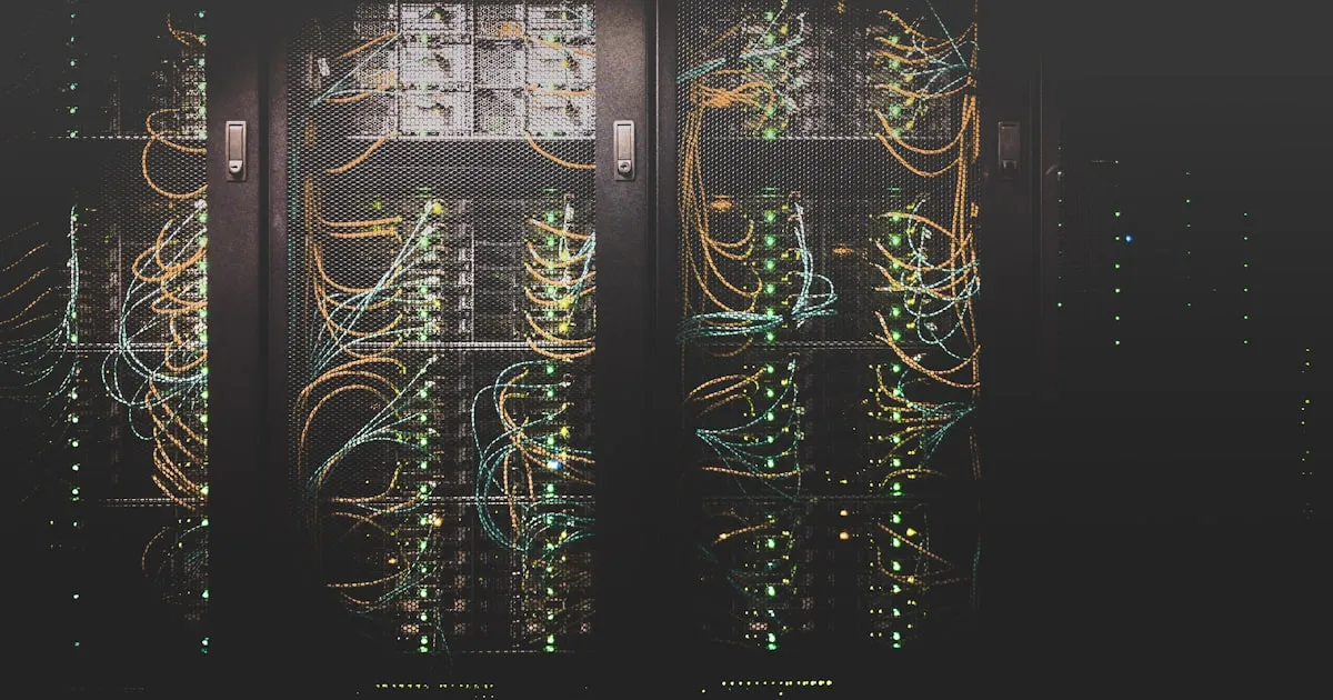
AI HARDWARE PCB FABRICATION
Building AI Infrastructure? Secure Your PCB Capacity Now.
We fabricate 16-30 layer boards for AI accelerators with dedicated capacity allocations. Lock in lead times before the H2 2026 demand surge hits.
Get Capacity Quote ›The Google TPU Factor: Why It Matters
Google’s TPU program becoming the largest single source of AI-PCB demand by 2028 represents a structural shift in the market. Unlike Nvidia’s GPU ecosystem — where demand flows through multiple OEM partners and add-in-card manufacturers — Google’s TPU procurement is centralized and driven by a single customer with massive volume commitments.
For the PCB supply chain, this concentration creates both opportunity and risk. The opportunity is obvious: $16 billion in TPU PCB procurement represents massive order volumes for qualified suppliers. The risk is that a single customer shifting their procurement strategy or experiencing demand softening can ripple through the entire supply chain simultaneously.
The PCB technical requirements for TPU carrier boards and their associated switch/interconnect infrastructure overlap significantly with GPU boards: high layer count, heavy copper power delivery, and tight impedance control on high-speed interfaces. Manufacturers already building GPU boards can potentially capture TPU orders without significant capital investment — but qualification cycles for Google’s supply chain are notoriously rigorous.
Optical Module PCBs: The Fastest-Growing Segment
The 135-178% annual growth in optical module PCB demand deserves specific attention because this segment has different fabrication requirements than compute boards.
Optical module substrates are typically:
- Thin profile (0.8-1.2mm total thickness)
- Moderate layer count (8-14 layers)
- Tight impedance tolerance (+/-5% or better on 50GHz+ channels)
- Low-loss laminate materials (Dk below 3.0, Df below 0.002 at 28GHz)
- Fine trace/space (3/3mil or tighter for 112G PAM4 channels)
- Small form factor (high panel utilization, many units per panel)
This is fundamentally different from the thick, heavy-copper, high-layer-count GPU carrier boards. A manufacturer optimized for one may not have the process controls optimized for the other. The surging optical demand creates opportunity for fabricators with fine-line capabilities and low-loss material expertise.
At AtlasPCB, our high-frequency PCB capabilities include processing of ultra-low-loss laminates with impedance tolerances to +/-5%, which aligns with optical module substrate requirements. We have seen a 3x increase in RFQs for optical transceiver substrates in Q2 2026 compared to Q4 2025.
Supply Chain Implications: The 18-Month Materials Bottleneck
Perhaps the most concerning finding in Citi’s report is the upstream materials constraint. While PCB manufacturers can expand from greenfield to production in 13-15 months, the upstream supply chain for copper-clad laminates (CCL) and fiberglass cloth requires 18+ months for meaningful capacity additions.
This creates a sequential bottleneck: even when new PCB fab capacity comes online in 2027, it may face constrained material supply if CCL manufacturers have not invested in parallel. The implication for hardware programs with 2027-2028 production timelines is clear — material availability may become the binding constraint on PCB delivery, not fabrication capacity.
For engineers and procurement teams planning today, the actionable takeaway is to specify standard, widely-available materials wherever technically possible. Exotic low-loss laminates and specialty prepregs will face the tightest supply, while mainstream high-Tg FR-4 variants (Shengyi S1000-2M, ITEQ IT-180A) have broader supply bases and more headroom for demand growth.
ATLASPCB
Concerned About AI-PCB Supply Tightening? Talk to Our Material Sourcing Team.
We maintain direct relationships with 6 laminate suppliers and can confirm material availability before you commit your design. Get realistic lead times, not optimistic promises.
Check Material Availability ›Reviewed by AtlasPCB Engineering Team — 15+ years in advanced PCB fabrication for RF, HDI, and rigid-flex applications.
Related Reading:
About AtlasPCB — We specialize in complex PCB manufacturing for HDI, RF, and high-reliability applications. Explore our full PCB manufacturing capabilities, or get an instant online quote . Every order includes free engineering review. Get your quote.
Reviewed by AtlasPCB Engineering Team — IPC-certified manufacturing specialists with 15+ years of production experience in HDI, RF, and high-reliability PCB fabrication. Content based on factory floor data and real customer design reviews.
- AI PCB
- market forecast
- Google TPU
- PCB demand
- industry news