· AtlasPCB Engineering · Industry News · 7 min read
AT&S Invests EUR 2 Billion in Malaysia AI Substrate Expansion — What It Means for PCB Buyers
AT&S announces EUR 1.5-2.0 billion investment in Kulim, Malaysia for AI substrate capacity with AMD partnership. Analysis of supply chain impact, substrate availability timeline, and implications for PCB procurement in 2026-2028.
The Investment at a Glance
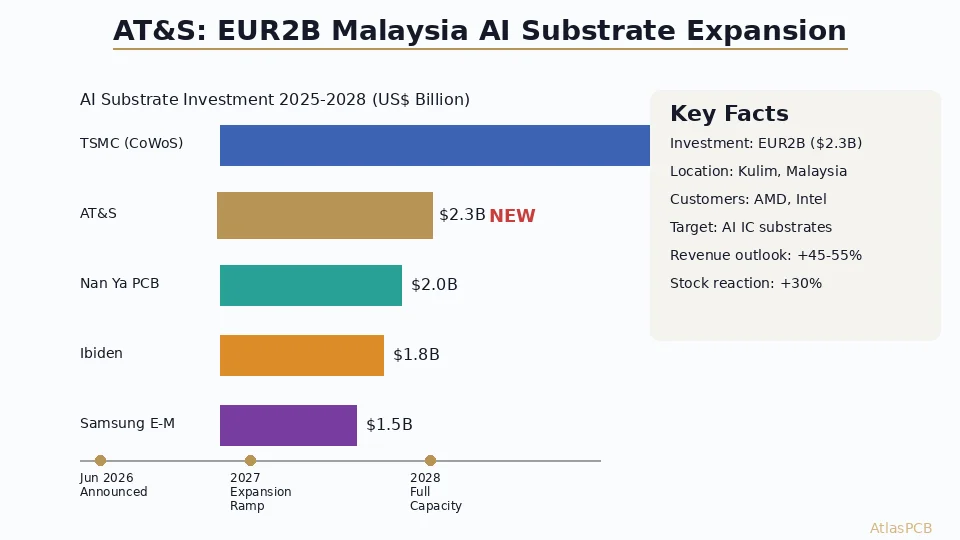
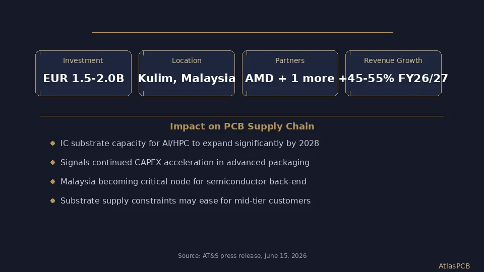
Austrian IC substrate and PCB manufacturer AT&S announced on June 15, 2026 a landmark investment of EUR 1.5-2.0 billion (approximately US$1.74-2.32 billion) to expand high-end IC substrate capacity at its Kulim, Malaysia complex. The expansion is backed by long-term procurement commitments from AMD and at least one other unnamed leading technology company, financing the build through guaranteed demand rather than speculative capacity.
The immediate market reaction was dramatic—AT&S shares surged nearly 30% following the announcement—reflecting investor confidence that the AI infrastructure buildout is far from saturating. AT&S simultaneously raised its FY2026/27 financial outlook, now expecting revenue growth of 45-55% (up from 30-35%) and EBITDA margin of 32-37% (up from 25-29%), with capital expenditure lifted to EUR 1.0-1.2 billion from a previous EUR 400 million guidance.
This is not a speculative bet. The customer-backed financing structure means AMD and its unnamed partner have committed to purchasing the substrate output before a single panel runs through the new lines. For the broader electronics supply chain, this confirms what procurement teams have been experiencing for eighteen months: AI substrate demand is growing faster than the industry can build capacity.
Why Substrates Are the Bottleneck in AI Hardware
The AI accelerator supply chain has a well-documented constraint hierarchy: advanced packaging (CoWoS, HBM integration) sits at the tightest point, with IC substrates forming the second critical bottleneck. Every AI GPU, every HBM stack, every high-performance compute chiplet requires a substrate that routes thousands of signals between the silicon die and the PCB motherboard. These substrates use ABF (Ajinomoto Build-up Film) technology with feature sizes approaching 2/2 micron line/space—processing complexity that rivals front-end wafer fabrication.
AT&S, along with Japanese competitors Ibiden and Shinko, controls roughly 60% of the global ABF substrate market for advanced processors. When AT&S announces a EUR 2 billion expansion specifically for AI substrates, it reveals two things: first, that their existing capacity is fully sold out to AI customers through their current planning horizon; second, that customer demand visibility extends far enough into the future to justify billion-euro capital commitments with multi-year payback periods.
For PCB buyers who do not operate in the AI accelerator space, the substrate investment has cascading effects. Engineering talent, raw materials (ABF film, low-loss laminates, ultra-thin copper foil), and fabrication equipment are all shared resources between substrate and advanced PCB manufacturing. When substrate makers absorb these resources at premium prices, the supply available for conventional HDI and multilayer PCBs tightens accordingly.
SUPPLY CHAIN RESILIENCE
Secure Your HDI and Multilayer PCB Supply
While substrate makers pivot to AI, AtlasPCB maintains dedicated capacity for HDI up to 5+N+5 and multilayer boards up to 30 layers. No allocation conflicts with substrate production.
Check Lead Times ›Malaysia’s Rise as the Back-End Semiconductor Hub
The choice of Kulim, Malaysia for this expansion is strategic, not coincidental. Malaysia has emerged as the critical geography for semiconductor back-end operations—packaging, testing, and substrate manufacturing. Intel, Infineon, ASE, and now AT&S all operate major advanced packaging facilities in the Kulim Hi-Tech Park industrial zone. The concentration creates a supply chain ecosystem with shared logistics, trained workforce, and government incentives specifically targeting high-value semiconductor manufacturing.
For AT&S, expanding in Kulim rather than building new capacity in Austria or China offers several advantages: proximity to OSAT (outsourced semiconductor assembly and test) customers who receive the substrates, access to Malaysia’s semiconductor workforce pipeline, favorable tax incentives under MIDA (Malaysian Investment Development Authority) programs, and geographic diversification away from geopolitical risk in their Chongqing, China facility.
The broader trend is unmistakable. In the past twelve months, substrate and advanced PCB investment announcements in Southeast Asia have exceeded $8 billion—more than the previous five years combined. This geographic shift has direct implications for logistics-sensitive PCB buyers who previously sourced exclusively from Taiwan, China, or Japan. New capacity in Malaysia creates alternative supply options with potentially shorter shipping times to customers in India, the Middle East, and Oceania.
Impact Timeline for PCB Procurement Teams
Now through Q4 2026: No relief. The announcement confirms existing capacity is fully allocated. ABF substrate lead times remain at 16-24 weeks. Advanced HDI PCB lead times stay elevated (3-5 weeks for complex builds). Material costs for low-loss laminates and ultra-thin copper foils remain at 2025 elevated levels.
H1 2027: Marginal improvement as AT&S qualifies initial lines and ramps pilot production. However, AMD and the unnamed partner hold first allocation rights, meaning merchant market availability does not materially improve. Expect AT&S to begin declining some conventional PCB orders to prioritize substrate output.
H2 2027 - 2028: Meaningful capacity addition comes online. Substrate allocation constraints should begin easing for second-tier customers. Some material pricing pressure may subside as increased demand for ABF film, CCL, and copper foil is met by suppliers who have also been expanding (Ajinomoto, Resonac, Mitsui Mining). For PCB buyers outside the AI segment, lead time normalization begins.
2028+: The supply-demand balance for AI substrates should approach equilibrium assuming no further acceleration in AI deployment rates. However, next-generation AI architectures (chiplets requiring larger substrates, optical interconnect integration) could sustain the demand-supply gap.
NO SUBSTRATE CONFLICT
Dedicated PCB Fabrication — Not Competing with AI Substrates
Our factory capacity is 100% dedicated to PCB fabrication. No substrate lines, no allocation conflicts. Your lead times are our lead times.
Get Instant Quote ›What This Means for Hardware Engineers Ordering PCBs Today
If you are designing boards that use HDI construction, advanced materials, or high layer counts, the AT&S announcement reinforces several procurement strategies worth adopting now:
Lock in material early. High-Tg laminates, low-loss materials, and ultra-thin copper foils are shared between substrate and PCB manufacturing. Place material reservations for production builds 8-12 weeks ahead rather than the traditional 4-6 weeks. Your PCB fabricator can hold material allocation against confirmed orders.
Qualify alternative fabricators. If your current supplier has substrate production alongside PCB lines, they may deprioritize your PCB orders as substrate demand grows. Having a qualified backup fabricator focused purely on PCB production—without substrate capacity conflict—provides supply security.
Design for available materials. Where possible, use standard-thickness laminates and common copper weights that fabricators stock in volume. Non-standard constructions that require special material orders add weeks to an already-tight supply chain.
The AT&S investment is fundamentally positive for the electronics industry—more substrate capacity means more AI hardware can ship, which drives demand for all the PCBs, connectors, and passives that surround AI accelerators. But during the 18-24 month buildout period, procurement teams must actively manage supply risk rather than assuming business-as-usual lead times.
ATLASPCB
Stable Lead Times. No Substrate Allocation Conflicts.
Get your multilayer and HDI boards without competing against AI substrate demand. Upload Gerbers for a quote with confirmed material availability.
Upload Gerber Files ›Related Reading:
About AtlasPCB — We specialize in complex PCB manufacturing for HDI, RF, and high-reliability applications. Explore our full PCB manufacturing capabilities, or get an instant online quote . Every order includes free engineering review. Get your quote.
Reviewed by AtlasPCB Engineering Team — IPC-certified manufacturing specialists with 15+ years of production experience in HDI, RF, and high-reliability PCB fabrication. Content based on factory floor data and real customer design reviews.
- AT&S
- IC substrate
- AI
- Malaysia
- AMD
- supply chain
- PCB industry
- advanced packaging