· David Okafor · Engineering · 11 min read
Aspect Ratio Limits in PCB Drilling: How Hole Depth Affects Reliability
A fabrication engineer's guide to PCB drill aspect ratio constraints, explaining how board thickness and hole diameter interact to determine plating quality, registration accuracy, and long-term via reliability in multilayer designs.
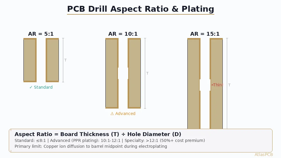
Every multilayer PCB design eventually confronts the physics of drilling: the deeper the hole relative to its diameter, the more difficult it becomes to achieve uniform copper plating, maintain positional accuracy, and ensure long-term reliability under thermal cycling. This relationship, expressed as the aspect ratio — board thickness divided by drilled hole diameter — is one of the most fundamental constraints in PCB fabrication, yet it remains poorly understood by many designers who specify vias based on electrical requirements alone without considering manufacturability implications. Drawing on our experience drilling and plating hundreds of thousands of holes daily across board thicknesses from 0.8 millimeters to 6.0 millimeters, this article explains what happens inside a drilled hole as aspect ratios increase, where the practical limits lie for different fabrication processes, and how designers can specify vias that achieve their connectivity objectives without compromising reliability.
Defining Aspect Ratio in Context
The aspect ratio of a drilled hole is calculated by dividing the board thickness by the finished hole diameter. A 1.6 millimeter thick board with a 0.3 millimeter drilled hole has an aspect ratio of 5.3:1. A 3.2 millimeter thick board with the same 0.3 millimeter hole has an aspect ratio of 10.7:1 — and the fabrication challenges are dramatically different despite using the same drill bit.
It is important to distinguish between drilled hole diameter and finished hole diameter when calculating aspect ratios for DFM purposes. The drilled hole is always larger than the finished hole because electroplated copper reduces the opening. For a target finished hole of 0.25 millimeters with 25 micrometers of copper plating per side, the drilled hole must be 0.30 millimeters. The aspect ratio that matters for plating chemistry is based on the drilled hole diameter (the hole as it exists during the plating process), while the aspect ratio relevant to electrical performance uses the finished diameter.
In our facility, we classify aspect ratios into three practical categories that govern process selection and capability. Standard aspect ratios below 8:1 can be processed through our conventional horizontal plating lines with standard chemistry and achieve IPC Class 2 and Class 3 requirements without special measures. Enhanced aspect ratios between 8:1 and 12:1 require modified plating parameters, extended plating times, and may necessitate pulse plating or reverse pulse techniques to achieve adequate throwing power. Extreme aspect ratios above 12:1 demand dedicated vertical plating cells with specialized high-throwing-power chemistry, careful process monitoring, and typically increase cost by 30 to 50 percent compared to standard processing.
The Physics of Plating Distribution
The fundamental challenge of high aspect ratio plating is delivering fresh copper ions to the bottom and center of a deep, narrow hole while simultaneously managing hydrogen gas evolution that can block fluid exchange. In a conventional acid copper plating bath, copper ions are consumed at the cathode surface (the hole wall) and must be replenished by diffusion and convection from the bulk solution. At low aspect ratios, agitation of the plating solution provides adequate mass transport throughout the hole. As the aspect ratio increases, the narrow opening restricts fluid flow into the hole interior, creating a diffusion-limited zone at the hole center where plating rate decreases relative to the surface and hole opening.
This phenomenon produces the characteristic plating distribution seen in high aspect ratio holes: thicker copper at the hole entrance tapering to thinner copper at the center of the hole barrel. IPC-6012 expresses this as the “throwing power” requirement, specifying that the minimum copper thickness at the hole center must not fall below specified values depending on the Class level. For Class 2 products, minimum barrel copper is 20 micrometers. For Class 3 high-reliability products, minimum barrel copper increases to 25 micrometers. Meeting these minimums at the hole center while controlling maximum copper buildup at the surface (which affects impedance and etch uniformity) becomes progressively more challenging as aspect ratios increase.
Our cross-sectional analysis data from production lots demonstrates this clearly. At aspect ratios of 6:1, typical copper distribution shows surface-to-center ratios of 1.2:1 to 1.4:1, meaning the center copper is 70 to 85 percent of the surface copper thickness. At 10:1, this ratio degrades to 1.6:1 to 2.0:1, with center copper representing only 50 to 60 percent of surface thickness. At 14:1, achieving even 40 percent center-to-surface ratios requires specialized chemistry with suppressor-accelerator-leveler additive systems specifically formulated for high-throw applications.
The practical consequence for designers is straightforward: specifying higher aspect ratios requires accepting either thicker surface copper (which reduces etch resolution for fine traces) or investing in more expensive plating processes that maintain distribution at acceptable surface thicknesses. Neither option is free, and understanding this trade-off early in the design process prevents costly respins.
Drill Bit Behavior at Depth
Beyond plating, the drilling process itself becomes more challenging at higher aspect ratios. A mechanical drill bit advancing into a deep hole experiences increasing wall contact friction, reduced chip evacuation efficiency, and progressive positional drift. The drill bit behaves somewhat like a long cantilever beam — as the unsupported length increases relative to the diameter, lateral deflection becomes more pronounced. This deflection manifests as positional inaccuracy at the bottom of the hole relative to the entry point, a phenomenon called drill wander.
For standard carbide micro-drills operating at 0.3 millimeters diameter in FR-4 material, our process data shows positional accuracy of plus or minus 25 micrometers for boards up to 2.0 millimeters thick (aspect ratio 6.7:1). At board thicknesses above 3.0 millimeters with the same drill (aspect ratio 10:1), positional spread increases to plus or minus 50 micrometers, with occasional outliers reaching 75 micrometers. This positional uncertainty directly impacts annular ring requirements — designers must allocate larger pad sizes to maintain minimum annular ring compliance at all layers, consuming valuable routing real estate.
Chip evacuation compounds the challenge. Drill flutes must carry cut material (chips) back up and out of the hole. In deep holes, chips can pack in the flutes, generating heat through friction and causing drill breakage or smeared resin on the hole wall. Smeared resin prevents copper from adhering to the glass-reinforced substrate during plating, creating the dreaded condition known as barrel cracking under thermal stress. Our process engineering team addresses this through controlled peck drilling cycles at high aspect ratios, where the drill retracts periodically to clear chips before advancing further. This cyclic drilling extends hole quality at the expense of throughput — a 12:1 aspect ratio hole may require three to four peck cycles compared to a single plunge for a 6:1 hole, effectively tripling drilling time.
Registration and Annular Ring Impact
The registration between drilled holes and copper pads on inner layers depends on multiple factors: drill accuracy, layer-to-layer alignment during lamination, material dimensional stability, and scaling compensation applied during imaging. As board thickness increases, the lamination pressure required to consolidate many layers introduces additional registration uncertainty, particularly for layers far from the core reference point.
For a 20-layer board at 3.0 millimeters thickness drilled with 0.3 millimeter holes (10:1 aspect ratio), the cumulative registration budget typically breaks down as: drill position accuracy plus or minus 50 micrometers, lamination registration plus or minus 50 micrometers, artwork scaling tolerance plus or minus 25 micrometers. The root-sum-square combination gives approximately plus or minus 75 micrometers of total registration uncertainty. Meeting IPC Class 3 minimum annular ring requirements of 50 micrometers on all internal layers demands pad diameters at least 0.55 millimeters for a 0.3 millimeter finished hole — significantly larger than the minimum pad sizes many designers specify.
Our DFM review team regularly encounters designs where engineers have specified 0.45 millimeter pads for 0.25 millimeter finished holes on 16 to 20 layer boards exceeding 2.5 millimeters thickness. While this meets the geometric minimum annular ring requirement when all features are perfectly aligned, it leaves zero margin for the registration stack-up described above. The result is annular ring violations on inner layers that either require scrapping the panel or requesting a customer waiver — neither outcome is desirable for schedule or cost.
Reliability Under Thermal Cycling
The aspect ratio of a via determines its vulnerability to failure under thermal cycling. When a PCB assembly experiences temperature excursions during operation or reflow, differential expansion between the copper via barrel and the surrounding FR-4 dielectric creates axial stress along the via barrel. The via barrel acts as a copper tube embedded in an expanding matrix — as the board thickness expands in the Z-direction during heating (FR-4’s coefficient of thermal expansion in Z is typically 50 to 70 ppm per degree Celsius above Tg), the barrel must stretch to accommodate this expansion.
For a 1.6 millimeter thick board experiencing a temperature rise from 25 to 260 degrees Celsius during reflow, the Z-axis expansion is approximately 40 to 55 micrometers. The copper barrel must absorb this strain without cracking. At aspect ratios below 8:1, the copper barrel has sufficient cross-sectional area (relative to its length) to distribute this strain without exceeding its fatigue endurance limit over thousands of thermal cycles. As aspect ratios increase beyond 10:1, the barrel becomes longer and relatively thinner at its center, concentrating stress at the weakest plating region and reducing fatigue life.
Interconnect stress testing (IST) data from our reliability qualification program quantifies this relationship. Standard IPC test vehicles fabricated at our facility with aspect ratios of 6:1 consistently survive 500 or more thermal cycles from room temperature to 260 degrees Celsius without failure. Identical constructions at 10:1 show first failures appearing between 200 and 350 cycles. At 14:1, even optimized plating processes yield first failures between 100 and 200 cycles. These numbers inform the reliability budgets for high-rel applications where field life of 20 years requires surviving thousands of operational thermal cycles at much lower temperature excursions.
Process Solutions for High Aspect Ratios
When design requirements demand aspect ratios above 10:1, several fabrication techniques can maintain reliability within acceptable limits. The most common approach in our facility is specifying heavier copper plating — building up 35 or 50 micrometers of barrel copper instead of the standard 25 micrometers. The additional copper provides greater fatigue endurance by distributing thermal stress over a larger cross-sectional area. The trade-off is increased plating time, higher material cost, and reduced finished hole diameter (requiring a larger initial drill to maintain the target finished hole size, which partially defeats the purpose of using smaller vias).
Pulse plating and periodic pulse reverse (PPR) plating represent more sophisticated solutions. By applying current in controlled pulses rather than continuous DC, the mass transport limitation at the hole center is partially overcome. During the off-time between pulses, copper ion concentration at the hole center replenishes through diffusion. Reverse pulses preferentially remove copper from high-current-density areas (the hole opening), redistributing material toward the center. Our PPR-capable lines achieve center-to-surface ratios of 70 to 80 percent at 12:1 aspect ratios, compared to 50 to 60 percent with conventional DC plating.
For extreme applications above 14:1, we recommend design alternatives that avoid the single deep hole entirely. Sequential lamination with staggered vias connects the same layers through two or more shorter via segments, each with manageable aspect ratios. A 4.0 millimeter thick board that would require a 14:1 ratio for a through-hole via can instead use a combination of blind vias, buried vias, and micro-vias that individually maintain ratios below 8:1. The additional lamination cycles add cost and lead time but deliver dramatically superior reliability for mission-critical applications.
DFM Guidelines for Designers
Based on our fabrication data and reliability testing, we recommend the following design approach for via specification in multilayer PCBs. For standard-reliability products (IPC Class 2, consumer electronics, networking equipment), maintain aspect ratios at or below 10:1 using the actual board thickness and drilled hole diameter. For high-reliability products (IPC Class 3, automotive, industrial, medical), maintain aspect ratios at or below 8:1. For extreme-reliability products (Class 3A, aerospace, defense, implantable medical), maintain aspect ratios at or below 6:1 or employ sequential lamination constructions.
When aspect ratio constraints prevent using the desired via size, consider several alternatives before requesting a capability exception. Increasing the drill size by 0.05 millimeters can drop the aspect ratio by a full point, dramatically improving plating distribution with minimal impact on routing density for most designs. Specifying a thinner board construction, where electrically acceptable, reduces both aspect ratio and material cost. Transitioning from through-hole vias to blind or buried vias where connections do not need to span the full board thickness keeps each individual via segment within manageable ratios.
Communication with your fabricator during the design phase — rather than after Gerber release — prevents the costly discovery that a chosen via structure requires extraordinary processing. A brief DFM consultation at the stackup definition stage costs nothing and can save weeks of delay and thousands of dollars in respins.
Reviewed by AtlasPCB Engineering Team
ATLASPCB DFM REVIEW
Free DFM Check on Your Next Design
Upload your Gerbers and our engineering team will verify aspect ratios, annular rings, and plating feasibility before production — no charge, no obligation.
Upload Design for Review ›About AtlasPCB — We specialize in complex PCB manufacturing for HDI, RF, and high-reliability applications. Explore our multilayer PCB fabrication up to 30 layers, or get an free engineering DFM review . Every order includes free engineering review. Get your quote.
Reviewed by AtlasPCB Engineering Team — IPC-certified manufacturing specialists with 15+ years of production experience in HDI, RF, and high-reliability PCB fabrication. Content based on factory floor data and real customer design reviews.
- DFM
- PCB drilling
- aspect ratio
- via reliability
- multilayer PCB
- plating