· AtlasPCB Engineering Team · Engineering · 11 min read
Buried and Blind Via Reliability: Aspect Ratio Limits, Plating Uniformity, and IPC Class 3 Requirements
Deep technical analysis of buried and blind via reliability covering aspect ratio limits, plating void risks, cross-section quality, and IPC Class 3 compliance for HDI PCBs.
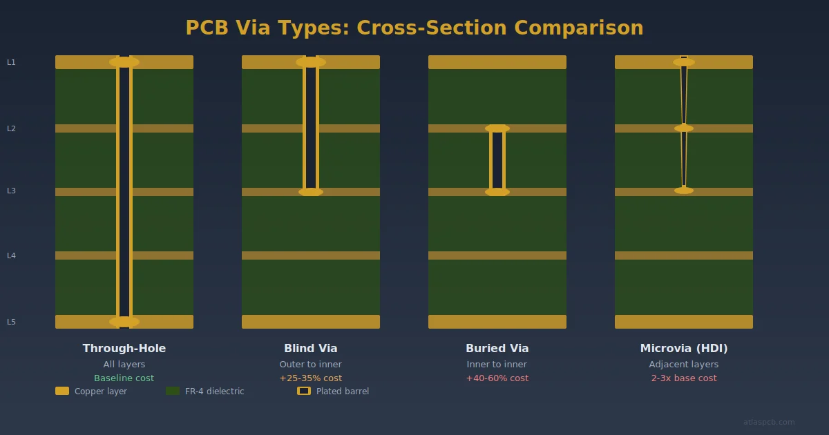
High-density interconnect technology has transformed PCB design from a relatively straightforward process of routing traces between through-hole vias into a three-dimensional puzzle where signal and power connections must navigate through blind vias, buried vias, and microvias across multiple lamination cycles. The reliability of these interconnect structures, particularly for applications governed by IPC-6012 Class 3 or Class 3A requirements, depends on manufacturing parameters that are far more challenging to control than those of conventional through-hole vias. Understanding the physics of copper electroplating within high-aspect-ratio blind holes, the thermal stress mechanisms that drive via fatigue, and the inspection methods that verify structural integrity is essential for designers who specify HDI technology in their products.
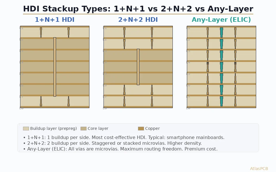
In our HDI production lines, we fabricate boards with up to six sequential lamination cycles, incorporating stacked and staggered microvias, buried vias that span multiple core layers, and blind vias drilled from external surfaces into interior layers. Each via type presents distinct manufacturing challenges, and the reliability of the finished product depends on the interaction between design choices, material properties, and process control at each lamination stage. This article examines the reliability considerations for buried and blind vias in detail, providing the technical depth needed to make informed design decisions for high-reliability applications.
Aspect Ratio: The Fundamental Constraint
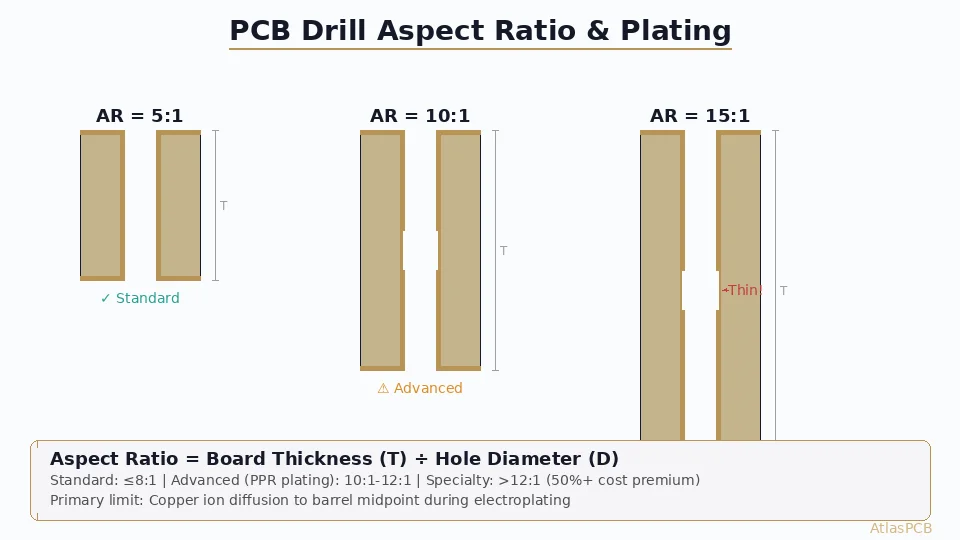
The aspect ratio of a via, defined as the ratio of its depth to its drilled diameter, is the single most important parameter governing plating reliability. Copper electroplating must deposit a uniform metal layer along the entire length of the via barrel, from the surface opening down to the bottom of a blind via or through the full depth of a buried via. As the aspect ratio increases, the electroplating chemistry faces increasing difficulty transporting fresh copper ions to the deepest regions of the via while removing depleted solution.
For blind vias, the aspect ratio challenge is compounded by the closed-end geometry. A blind via drilled 0.15 mm deep with a 0.2 mm diameter has an aspect ratio of 0.75:1, which represents a practical manufacturing limit for conventional mechanical drilling and electroplating processes. At this ratio, the plating solution must penetrate to the bottom of a hole that has only one opening, relying on diffusion and convective agitation to maintain adequate ion concentration throughout the via depth. The bottom corner where the via barrel meets the target pad is particularly vulnerable to plating voids because the geometry creates a stagnant zone where fresh plating solution has difficulty reaching.
Buried vias, which are plated before lamination as part of an inner core fabrication step, generally achieve more reliable plating because they are through-vias within the individual core being processed. A buried via connecting layers 3 and 4 in a core that is 0.2 mm thick with a drill diameter of 0.15 mm has an aspect ratio of 1.33:1, which is well within the capability of standard plating processes. However, the reliability challenge for buried vias shifts from plating quality to structural integrity during subsequent lamination cycles, where temperature and pressure can create stress concentrations at the via barrel interfaces.
Plating Uniformity and Void Formation
The uniformity of copper plating within a blind or buried via directly determines its current-carrying capacity and its resistance to thermal fatigue. IPC-6012 Class 3 requires a minimum copper plating thickness of 20 micrometers at any point within the via barrel, with no voids exceeding defined size limits. Achieving this minimum in the deepest portion of a high-aspect-ratio blind via requires sophisticated plating chemistry and process control that goes well beyond standard through-hole plating.
Modern pulse plating and periodic reverse plating techniques significantly improve the throwing power of the electroplating process in high-aspect-ratio features. By alternating between plating pulses that deposit copper and brief reverse pulses that preferentially dissolve copper at the surface opening, the process can achieve a more uniform deposit from top to bottom. The plating bath additives, including suppressors, accelerators, and levelers, work synergistically with the pulse waveform to control deposition rate as a function of position within the via.
In our production process, we monitor plating uniformity through regular cross-section analysis of test coupons that are processed alongside production panels. These coupons contain blind vias at the design aspect ratio, and we measure the copper thickness at multiple points along the via barrel: the surface, the mid-depth, and the bottom. Our process specification requires that the ratio of minimum to maximum copper thickness within any via, known as the throwing power ratio, exceeds 0.7 for Class 3 compliance. In practice, our optimized plating process achieves throwing power ratios of 0.75 to 0.85 for aspect ratios up to 0.75:1, providing comfortable margin against the minimum thickness requirement.
Plating voids represent the most serious reliability risk in blind and buried vias. A void in the copper barrel creates a discontinuity that acts as a stress concentrator during thermal cycling. The CTE mismatch between the copper barrel and the surrounding dielectric causes the via to experience compressive stress during heating and tensile stress during cooling. At a void, the local stress concentration can exceed the fatigue strength of the copper, initiating a crack that propagates around the barrel circumference during subsequent thermal cycles until the via electrically fails.
From our failure analysis work, we have identified several root causes of plating voids in blind vias. Air entrapment during the plating immersion step, where an air bubble becomes trapped at the bottom of the blind hole, prevents plating solution from contacting the target pad surface. Inadequate desmear processing after laser drilling can leave residual resin on the target pad that prevents copper nucleation. Insufficient agitation during plating allows local depletion of copper ions at the via bottom. Each of these root causes requires specific process controls, and we have implemented automated monitoring systems that verify desmear completeness, solution agitation parameters, and immersion protocols to minimize void occurrence.
Sequential Lamination and Its Impact on Via Reliability
HDI boards with multiple lamination cycles subject buried vias to repeated thermal excursions during the lamination of subsequent layers. Each lamination cycle exposes the existing buried vias to temperatures of 180 to 200 degrees Celsius and pressures of 300 to 400 psi for durations of 60 to 90 minutes. The cumulative thermal exposure creates fatigue loading on the buried via structures that does not exist in simple two-sided boards.
The critical concern during sequential lamination is the differential thermal expansion between the buried via copper barrel and the surrounding dielectric. During the heating phase of lamination, the dielectric expands more in the Z-axis direction than the copper barrel, creating tensile stress on the barrel walls. If the copper has insufficient ductility, which can occur if the plating bath produces a high-stress deposit, the barrel can develop micro-cracks during lamination that become reliability weak points during product lifetime thermal cycling.
We have found through extensive thermal stress testing that the elongation properties of the electrodeposited copper are as important as the thickness for via reliability. IPC-6012 Class 3 requires a minimum copper elongation of 12 percent for inner layer foil, but this specification does not directly address the elongation of electroplated copper in via barrels. Through our own characterization work, we have established internal process specifications that require a minimum elongation of 15 percent for via barrel copper, measured on plating test strips processed alongside production panels. This enhanced ductility requirement provides margin for the cumulative thermal exposure inherent in sequential lamination processes.
Cross-Section Analysis and Quality Verification
Cross-sectional metallographic analysis remains the definitive method for verifying blind and buried via quality. The process involves mounting a sample in epoxy, grinding and polishing to expose the via cross-section at the approximate midplane, and examining the structure under optical microscopy at magnifications of 100 to 500 times. The cross-section reveals copper thickness, void presence, barrel crack initiation, pad connection quality, and dielectric condition around the via.
For production quality control, we perform cross-section analysis on test coupons from every production lot. The coupon design includes blind vias at the maximum aspect ratio used in the production design, placed at the center and edges of the panel to verify plating uniformity across the working area. Each cross-section is documented photographically and measured using calibrated image analysis software that reports copper thickness at defined measurement points.
IPC-6012 Class 3 specifies acceptance criteria for cross-section evaluation that include minimum copper thickness, maximum void size relative to barrel thickness, and pad connection quality. For blind vias, the target pad connection is particularly important: the copper must form a continuous metallurgical bond with the target pad foil, with no separation or delamination visible at the interface. Any visible separation, even without a complete void, is cause for rejection at Class 3 level because it indicates a potential nucleation site for fatigue crack growth during service life thermal cycling.
Beyond optical microscopy, we employ scanning electron microscopy for failure analysis when defects are identified. SEM provides higher resolution imaging that can reveal micro-cracks, grain boundary structures, and contamination layers that are invisible under optical magnification. Energy-dispersive X-ray spectroscopy performed in the SEM can identify chemical contamination at void surfaces, helping to determine root cause. For example, detection of sulfur compounds at a void surface suggests plating bath contamination, while detection of organic carbon suggests inadequate desmear.
Thermal Reliability Testing
The ultimate verification of via reliability is accelerated thermal cycling that simulates the product lifetime thermal exposure in a compressed time frame. IPC-TM-650, Method 2.6.26, defines the thermal stress test for printed board quality assessment, but many Class 3 applications require extended testing beyond the minimum IPC protocol.
Standard thermal cycling for via reliability evaluation subjects the test vehicle to cycles between minus 55 and plus 125 degrees Celsius, with a dwell time at each extreme and a transition time between extremes that creates the rate of temperature change seen in service. Resistance monitoring of daisy-chain via structures allows detection of crack initiation as a resistance increase, with failure typically defined as a 10 percent increase from the initial resistance value.
Our qualification testing for new HDI via designs subjects the test vehicles to 500 thermal cycles minimum for Class 3 equivalent qualification, with many aerospace and defense customers requiring 1,000 cycles before acceptance. We have accumulated a substantial database of thermal cycling results correlated with specific via geometries, plating parameters, and material systems that allows us to predict reliability performance for new designs based on the parametric similarity to previously tested structures.
Design Guidelines for Reliable Blind and Buried Vias
Based on our manufacturing experience and reliability testing database, we provide the following design principles for achieving reliable blind and buried via structures in Class 3 applications. The blind via aspect ratio should not exceed 0.75:1 for mechanically drilled vias or 1.0:1 for laser-drilled microvias where the smaller diameter allows more effective plating solution exchange. The target pad for a blind via should provide a minimum annular ring of 0.075 mm after registration tolerance allocation to ensure complete pad capture even with worst-case layer alignment.
Buried vias within individual cores should maintain aspect ratios below 6:1 for standard mechanical drilling and plating processes. For higher aspect ratios, advanced plating techniques or design modifications such as larger drill diameters become necessary. The copper weight on the core layers containing buried vias should be at least 0.5 ounce to provide adequate pad material for thermal cycling without pad pullaway.
Stacked microvias, where multiple blind via layers are aligned directly on top of each other, create a columnar copper structure that must maintain structural integrity through all sequential lamination cycles. IPC standards allow stacking of up to three microvia layers, but each additional stack level increases the cumulative thermal exposure and the associated reliability risk. For the highest reliability applications, staggered microvias offset from layer to layer provide more robust structures because each via connection is independently plated and inspected rather than relying on a continuous vertical copper column.
The interaction between via design, material selection, and process capability ultimately determines whether a blind or buried via will meet its reliability targets. At AtlasPCB, we approach each HDI design with a comprehensive evaluation of these interactions, providing customers with manufacturing feasibility assessments and reliability predictions based on our extensive production and testing experience. The goal is always to identify potential reliability risks during the design phase, when modifications are inexpensive, rather than discovering them during qualification testing or, worst of all, during field service.
About AtlasPCB — We specialize in complex PCB manufacturing for HDI, RF, and high-reliability applications. Explore our HDI PCB manufacturing capabilities, or get an full PCB manufacturing capabilities . Every order includes free engineering review. Get your quote.
Reviewed by AtlasPCB Engineering Team — IPC-certified manufacturing specialists with 15+ years of production experience in HDI, RF, and high-reliability PCB fabrication. Content based on factory floor data and real customer design reviews.
- Blind Vias
- Buried Vias
- HDI PCB
- IPC Class 3
- Via Reliability