· AtlasPCB Engineering Team · Engineering · 21 min read
PCB Copper Weight: Complete Selection Guide with Real Cost Data, DFM Constraints, and Current Capacity Tables
Definitive PCB copper weight guide covering oz/ft² to micron conversions, minimum trace/space per weight class, IPC-2152 current capacity data, mixed copper stackup strategies, real manufacturing cost multipliers, and a decision framework for selecting the right copper weight. Based on actual production data from thousands of boards.
Quick Answer
PCB copper weight is measured in ounces per square foot (oz/ft²), where 1oz equals 35 micrometers (1.4 mils) of copper thickness. Standard options range from 0.5oz (17.5µm) for signal-only boards to 6oz+ (210µm+) for extreme power applications. Selecting the right copper weight requires balancing current carrying requirements against DFM constraints — heavier copper demands wider traces and larger spacing due to etching undercut. For most mixed-signal designs, a hybrid stackup with 2oz outer layers for power distribution and 0.5oz inner layers for signal routing provides the optimal cost-performance balance, adding only 15-25% to the board cost versus all-1oz construction.
What PCB Copper Weight Actually Means
Copper weight is one of those PCB specifications that engineers inherit from decades-old convention without questioning the underlying logic. The term itself causes confusion because we are specifying a weight measurement — ounces — to describe what we actually care about: thickness. The convention originates from the copper foil manufacturing process where producers roll copper to a uniform thickness defined by the mass of copper distributed over one square foot of area. One ounce of copper spread over one square foot yields a foil thickness of approximately 35 micrometers, or 1.37 mils.
This measurement system persists because the PCB industry standardized around it long before metric conversion became common, and because laminate suppliers still sell copper-clad materials by copper weight designation. When you specify “1oz copper” on your fabrication drawing, the manufacturer knows you want 35 micrometers of base copper thickness on that layer — no further translation required.
Here is the complete conversion table that covers every standard copper weight you will encounter in PCB fabrication:
Half-ounce copper equals 17.5 micrometers, which is 0.7 mils or 0.0175 millimeters. One-ounce copper equals 35 micrometers at 1.4 mils or 0.035 millimeters. Two-ounce copper reaches 70 micrometers at 2.8 mils or 0.07 millimeters. Three-ounce copper measures 105 micrometers at 4.2 mils or 0.105 millimeters. Four-ounce copper comes to 140 micrometers at 5.5 mils or 0.14 millimeters. Five-ounce copper reaches 175 micrometers at 6.9 mils or 0.175 millimeters. Six-ounce copper tops out at 210 micrometers, measuring 8.3 mils or 0.21 millimeters.
Beyond 6oz, specialty fabricators can produce boards up to 20oz (700 micrometers), though these require completely different manufacturing processes and are priced as custom projects rather than standard fabrication.
Standard Copper Weight Options and Real-World Applications
Understanding which copper weight suits which application requires thinking about the actual current demands and thermal constraints of your design — not just following convention. From our manufacturing floor where we process boards across every copper weight class, here is how real designs distribute across the spectrum.
Half-ounce copper (17.5 micrometers) serves signal-only applications where current capacity is irrelevant and trace density is the priority. We see this primarily in smartphone HDI boards, memory modules, and high-density FPGA breakout boards where designers need 3-mil traces on inner layers. The thinner copper enables finer features because less material needs to be etched away, resulting in less undercut and more consistent trace geometries. Approximately 15 percent of the boards crossing our production line use 0.5oz copper on at least one layer.
One-ounce copper (35 micrometers) remains the industry default for general-purpose applications. Consumer electronics, IoT devices, standard computing hardware, and communication equipment overwhelmingly use 1oz copper on all layers. It provides adequate current capacity for most signal traces and moderate power distribution while maintaining reasonable DFM margins. About 60 percent of our production volume uses 1oz copper uniformly across all layers.
Two-ounce copper (70 micrometers) enters the picture when designs need more than 1.5A per trace without excessively wide routing. Power supply boards, LED driver circuits, motor control systems, telecom power distribution, and automotive body electronics commonly specify 2oz copper on power layers while potentially keeping signal layers at 1oz. This represents roughly 18 percent of our production.
Three-ounce copper (105 micrometers) marks the entry point of what the industry considers “heavy copper” manufacturing. At this weight, the fabrication process changes meaningfully — etching times increase substantially, lamination cycles require modification to prevent resin starvation, and drilling parameters need adjustment for the thicker copper surface. Industrial power supplies, EV charging circuits, battery management systems for large packs, and high-current motor drivers commonly require 3oz copper. This represents about 5 percent of our volume.
Four-ounce and above (140+ micrometers) enters specialized territory requiring modified processes throughout the entire fabrication flow. Welding equipment, power inverters for solar and industrial applications, high-power RF amplifiers, and railway traction electronics demand these extreme copper weights. We produce these boards on dedicated production lines with modified etching chemistry and extended processing cycles.
Base Copper vs Finished Copper: Why Your Board Is Not What You Ordered
One of the most common misunderstandings we encounter in design reviews involves the difference between base copper weight (what you specify) and finished copper thickness (what you actually receive on outer layers). This distinction matters for impedance calculations, current capacity estimates, and mechanical thickness tolerance budgets.
When you specify 1oz copper, the laminate supplier provides core material and prepreg with 1oz (35 micrometer) copper foil. This is your base copper. However, outer layers go through the electroplating process during pattern plating (the standard subtractive process for multilayer boards), which deposits an additional 20-30 micrometers of copper onto all exposed copper surfaces. This means your “1oz” outer layer actually measures 55-65 micrometers — effectively approaching 2oz thickness — after plating.
Inner layers do not receive this additional plating because they are already patterned before lamination. The copper on inner layers remains at its specified base weight. This asymmetry between inner and outer layer copper thickness has direct implications for your design.
For impedance calculations, your outer layer 1oz copper traces are actually sitting at approximately 1.7oz effective thickness after plating. If your impedance modeling assumes 1.4 mil copper thickness on outer microstrip traces but the actual finished copper is 2.0-2.4 mils, your calculated impedance will be slightly off. At our facility, we account for this in our impedance modeling by using finished copper thickness rather than base copper weight — and we see designs regularly where engineers have not accounted for this difference, leading to 3-5 ohm impedance deviations from target.
For impedance-controlled designs, we recommend always communicating with your fabricator using base copper weight for specification purposes while ensuring your impedance calculator uses finished copper thickness. Most reputable manufacturers (including us) will run impedance simulations with actual finished copper values regardless of what the customer’s stackup shows, but it avoids confusion during the review process.
The tolerance on finished copper thickness after plating is typically plus or minus 20 percent of the plated thickness. For a 1oz base copper outer layer with 25 micrometers of plating, expect finished copper between 52 and 68 micrometers. This tolerance range is one reason why tight impedance specifications (less than 5 percent tolerance) on outer layers require careful process control.
How Copper Weight Affects Your Design Constraints
The relationship between copper weight and minimum achievable features is governed by etching physics — specifically, the phenomenon of undercut. When chemical etchant dissolves copper to create your trace pattern, it does not attack only from the top surface. The etchant also attacks sideways beneath the etch resist, eating into the copper from both sides of the trace simultaneously. The deeper the etch must penetrate (thicker copper), the more sideways erosion occurs.
This lateral etching, called undercut, means that heavier copper requires designers to specify wider traces and larger spaces between traces to account for the material that will be removed laterally during etching. The ratio between vertical etch depth and horizontal undercut is called the etch factor, and it typically ranges from 2.5:1 to 3.5:1 for standard acid etching processes.
Here are the minimum trace width and spacing values we reliably manufacture at each copper weight, based on our production capability data across thousands of boards:
For half-ounce copper (17.5 micrometers): minimum trace width of 3 mil (0.075mm) with minimum space of 3 mil. This is the finest geometry we can consistently achieve in volume production with standard acid etching.
For one-ounce copper (35 micrometers): minimum trace width of 3.5 mil (0.09mm) with minimum space of 3.5 mil for standard process. Preferred minimum of 4/4 mil for reliable yield above 95 percent.
For two-ounce copper (70 micrometers): minimum trace width of 6 mil (0.15mm) with minimum space of 6 mil. Many fabricators require 8/8 mil at this weight — we achieve 6/6 with controlled process parameters, but yield drops to approximately 90 percent at these minimums.
For three-ounce copper (105 micrometers): minimum trace width of 8 mil (0.2mm) with minimum space of 8 mil. Preferred design target of 10/10 mil for manufacturing comfort and consistent yield.
For four-ounce copper (140 micrometers): minimum trace width of 10 mil (0.254mm) with minimum space of 10 mil. Preferred design target of 12/12 mil.
For five-ounce copper (175 micrometers): minimum trace width of 12 mil (0.3mm) with minimum space of 14 mil. At this weight, alkaline etching replaces acid etching for better etch factor.
For six-ounce copper (210 micrometers): minimum trace width of 14 mil (0.35mm) with minimum space of 16 mil.
These numbers represent what our production line achieves consistently. Many common DFM mistakes we flag in design reviews involve specifying trace widths appropriate for 1oz copper on layers that use 2oz or heavier copper. If your design requires both fine traces and heavy copper, a mixed copper weight stackup (discussed below) is usually the better solution.
The trapezoidal trace cross-section created by etching undercut also affects impedance calculations. A 1oz copper trace has a nearly rectangular cross-section where the top width is only 1-2 mils narrower than the bottom width. But a 3oz copper trace has a significantly trapezoidal profile where the top width might be 6-8 mils narrower than the bottom. Your impedance modeling tool must account for this trapezoidal geometry — using rectangular cross-section assumptions on heavy copper will overestimate impedance by 5-10 percent.
Copper Weight and Current Carrying Capacity
Current carrying capacity is the primary driver for selecting heavier copper weights. The fundamental relationship is straightforward: more copper cross-sectional area allows more current to flow for a given temperature rise. But applying this relationship correctly requires understanding the IPC-2152 framework, which replaced the older IPC-2221 nomographs that many engineers still reference.
IPC-2152 (released 2009, updated) provides current capacity data based on extensive experimental testing with boards in real thermal environments. The older IPC-2221 charts were derived from theoretical models and MIL-STD-275 data from the 1950s that significantly underestimated current capacity for external layers while overestimating it for internal layers.
Using IPC-2152 methodology, here is the current carrying capacity for common configurations with a 10-degree Celsius temperature rise above ambient, assuming an ambient of 25 degrees Celsius:
For outer layer traces with 1oz base copper (finished approximately 1.7oz after plating): a 10-mil trace carries approximately 1.2A, a 20-mil trace carries 2.0A, a 50-mil trace carries 3.8A, and a 100-mil trace carries 6.2A.
For outer layer traces with 2oz base copper (finished approximately 2.7oz): a 10-mil trace carries approximately 1.8A, a 20-mil trace carries 3.0A, a 50-mil trace carries 5.5A, and a 100-mil trace carries 9.0A.
For inner layer traces with 1oz copper (no plating addition): a 10-mil trace carries approximately 0.8A, a 20-mil trace carries 1.4A, a 50-mil trace carries 2.8A, and a 100-mil trace carries 4.5A.
For inner layer traces with 2oz copper: a 10-mil trace carries approximately 1.3A, a 20-mil trace carries 2.2A, a 50-mil trace carries 4.2A, and a 100-mil trace carries 6.8A.
The critical insight from this data: inner layers carry significantly less current than outer layers at the same trace width and copper weight because internal traces cannot dissipate heat as effectively, being sandwiched between insulating dielectric layers rather than having convective cooling from air on one side.
Temperature rise is not linear with current — it follows approximately a square relationship. Doubling the allowable temperature rise from 10 to 20 degrees Celsius increases current capacity by approximately 40 percent, not double. For high-reliability applications (aerospace, medical, automotive), many specifications limit temperature rise to 10 degrees Celsius. For consumer applications where a 30 or even 40-degree rise is acceptable, you can often use lighter copper than the conservative tables suggest.
Mixed Copper Weight Stackups: Optimizing Cost and Performance
One of the most powerful but underutilized strategies in PCB design is the mixed copper weight stackup, where different layers use different copper thicknesses optimized for their specific function. Rather than specifying uniform heavy copper throughout the board (expensive and constraining), a mixed approach puts heavy copper only where current capacity demands it.
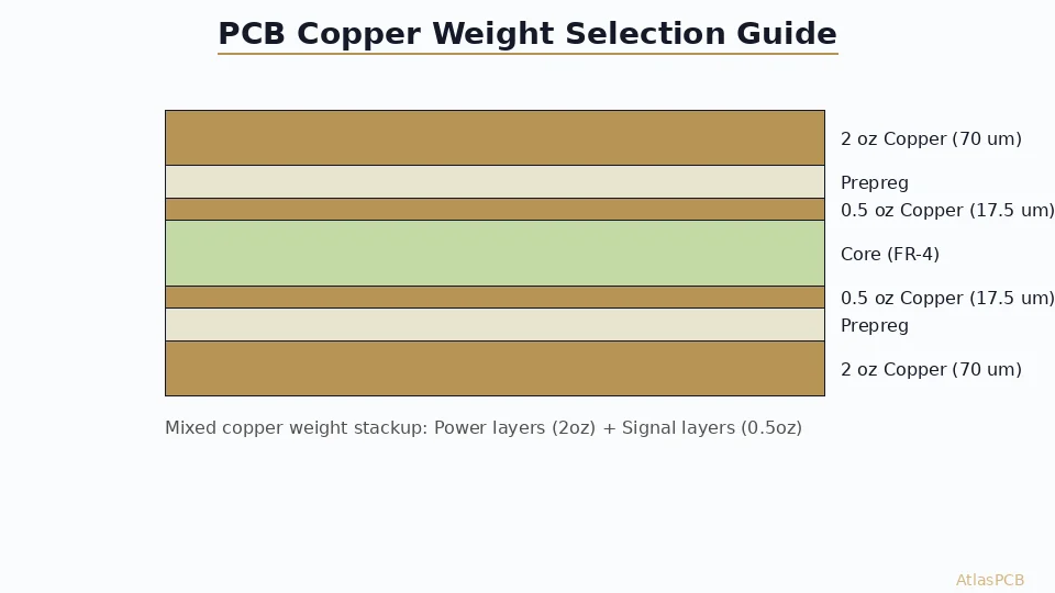
The most common configuration we manufacture is 2oz outer layers with 0.5oz or 1oz inner layers. This combination provides enhanced current capacity on outer power distribution traces (where components connect to power) while maintaining fine-pitch routing capability on inner signal layers. The cost premium over an all-1oz construction is typically 15-25 percent — far less than the 40-60 percent premium of using 2oz uniformly on all layers.
A more aggressive hybrid uses 3oz copper on two dedicated inner power planes while keeping signal layers at 0.5oz and outer layers at 1oz. This configuration works well for power converter designs where heavy currents flow through internal power and ground planes, but the outer layers primarily carry signal traces and component connections that do not need extreme current capacity. We see this frequently in telecom power supply designs and automotive ECU boards.
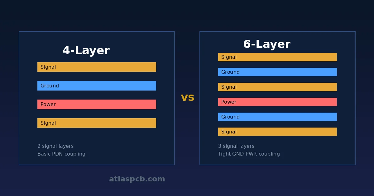
For a typical 4-layer board, a practical mixed stackup might look like this: Layer 1 (top signal/power) at 2oz, Layer 2 (ground plane) at 1oz, Layer 3 (power plane) at 1oz, Layer 4 (bottom signal/power) at 2oz. This gives you heavy copper where components attach and current enters the board, while internal planes at 1oz provide adequate power distribution for moderate current demands through their continuous copper pour area rather than trace current capacity.
The manufacturing complexity of mixed copper weight stackups is modest. We handle the different copper weights during the inner layer imaging and etching stage — different layers simply get different etch times. The lamination process accounts for the varying copper thicknesses in prepreg selection to maintain overall board thickness targets. The primary constraint is that mixed stackups require slightly more engineering time during CAM processing and may add one to two days to manufacturing lead time for first-article production.
Designers should note that mixed copper weight stackups affect impedance differently on each layer due to the varying copper thickness. We recommend specifying target impedance per layer and letting the manufacturer adjust dielectric thickness to hit targets, rather than rigidly specifying prepreg thickness and then finding impedance values are off.
Cost Impact: What Heavier Copper Actually Costs
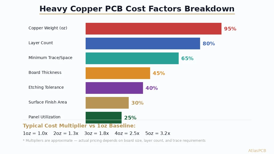
Every competitor article on copper weight says “heavier copper costs more” without providing actual numbers. Based on our production cost data across thousands of orders in 2026, here are real cost multipliers relative to a standard 1oz copper baseline for a typical 4-layer board at mid-volume (500-2000 pieces):
All layers at 0.5oz copper: 0.95x baseline (5 percent savings due to faster etching and slightly lower material cost, though this is partially offset by handling challenges with thinner copper).
All layers at 1oz copper: 1.0x (baseline). This is the reference point for all other calculations.
All layers at 2oz copper: 1.15-1.25x baseline (15-25 percent premium). The cost increase comes from roughly 40 percent higher material cost for 2oz copper foil, 60-80 percent longer etching cycles, and approximately 3-5 percent lower manufacturing yield.
Mixed stackup with 2oz outer and 1oz inner: 1.10-1.18x baseline (10-18 percent premium). This is consistently the most cost-effective approach for designs needing enhanced current capacity.
All layers at 3oz copper: 1.40-1.60x baseline (40-60 percent premium). At 3oz, the manufacturing process changes significantly — longer etch times, modified lamination cycles, reduced line productivity, and yield drops to 85-90 percent for typical designs.
All layers at 4oz copper: 1.80-2.20x baseline (80-120 percent premium). Four-ounce production requires dedicated processing time that disrupts standard production flow, alkaline etching rather than acid for some process steps, and careful lamination pressure profiles to prevent resin starvation.
All layers at 5-6oz copper: 2.50-3.50x baseline (150-250 percent premium). At these weights, boards enter our heavy copper production cell with different equipment, chemistry, and process parameters.
Beyond 6oz: quotation-based pricing that depends entirely on the specific design. Most orders in the 8-20oz range cost 4-8x the equivalent 1oz baseline.
These multipliers assume all other board parameters remain constant (same layer count, same board size, same quantity, same finish). In practice, designs requiring heavy copper often also need other premium features (thicker boards, high-Tg materials, extensive thermal management) that compound the cost increase.
The most impactful cost optimization we recommend to customers: if your design uses uniform 2oz copper across all layers but only two layers actually need the current capacity, switching to a mixed stackup (2oz on power layers, 1oz on signal layers) saves 5-10 percent immediately with zero performance compromise.
COPPER WEIGHT OPTIMIZATION
Get a DFM Review with Copper Weight Recommendations
Upload your design files and our engineering team will analyze your current requirements, recommend optimal copper weight per layer, and provide cost-optimized stackup options.
Upload Design Files ›
Heavy Copper PCB Manufacturing: Process Differences
The transition from standard copper weight (0.5-2oz) to heavy copper (3oz and above) is not merely a matter of longer etching — it requires fundamental changes across multiple manufacturing stages. Understanding these process differences helps explain the cost premiums and lead time extensions associated with heavy copper production.
Etching chemistry represents the most visible change. Standard PCB fabrication uses acid copper chloride (CuCl2) etchant operating at approximately 50 degrees Celsius with etch rates of 25-35 micrometers per minute. For 1oz copper, this means an etching cycle of approximately one to one-and-a-half minutes per side. For 3oz copper, the same chemistry would require four to five minutes — but the extended exposure degrades resist adhesion and amplifies undercut to unacceptable levels.
Heavy copper production (3oz and above) at our facility uses alkaline ammoniacal etchant (ammonia-based copper complexing agents) that provides a higher etch factor of 3:1 to 4:1 compared to the 2.5:1 to 3:1 typical of acid etching. The improved etch factor means less lateral undercut per unit of vertical etch depth, enabling tighter trace geometries than would be possible with acid chemistry on the same copper weight. However, alkaline etchant requires more careful temperature control, faster etch rate monitoring, and more frequent solution analysis.
Lamination is the second critical process change. Standard lamination uses prepreg resin flow to fill the gaps between copper traces and create a void-free dielectric layer. With heavy copper, the gap depth between traces is much deeper (a 3oz copper trace stands 105 micrometers proud, creating 105-micrometer-deep channels between features), requiring significantly more resin flow to fill without voids. This means either using higher resin-content prepregs (increasing material cost), using multiple prepreg sheets between heavy copper layers (increasing thickness and cost), or running modified lamination pressure profiles with slower ramp rates to allow adequate resin flow.
Resin starvation — where insufficient resin fails to completely fill the inter-trace channels — is the primary yield-killing defect in heavy copper lamination. We mitigate this through copper balancing (adding non-functional copper fills to equalize copper density across the panel), careful prepreg resin content selection based on the specific copper density distribution, and lamination recipe optimization specific to each heavy copper design. First articles typically receive cross-sectional analysis to verify complete resin fill before volume production proceeds.
Drilling heavy copper boards presents challenges because the drill bit must penetrate through thicker copper entry surfaces. Copper acts as an abrasive on carbide drill bits, accelerating wear and generating more heat at the hole entrance. For boards with 4oz or heavier copper on outer layers, we use aluminum entry material (backed by phenolic sheets) specifically designed for heavy copper, reduce drill hit counts per bit by 30-50 percent, and may use reduced spindle speeds on initial copper penetration.
Plating uniformity becomes more challenging with heavy copper because the deep channels between traces on outer layers create geometric plating distribution difficulties. The plating current density varies between the top of a trace (easy access to plating solution) and the bottom of a deep channel between traces (restricted access). Modified plating waveforms and agitation patterns compensate, but heavy copper boards generally show 15-20 percent more plating thickness variation than standard boards.
How to Choose the Right Copper Weight
Selecting copper weight should follow a systematic decision process based on actual current requirements rather than intuition or copying reference designs. Here is the framework we recommend to customers during design review consultations.
Start by identifying the maximum sustained current on each layer. Review your schematic for every power net and determine the maximum DC current that will flow through PCB traces (not through plane pours, which have effectively unlimited width). For each layer, identify the highest-current trace and the trace width you have allocated for it in your layout.
Using IPC-2152 data with your acceptable temperature rise (typically 10 degrees for high-reliability, 20-30 degrees for consumer), determine whether your allocated trace width can carry the required current at each copper weight option. If a 20-mil trace on 1oz outer copper carries your maximum current with acceptable temperature rise, there is no electrical reason to use heavier copper.
For current requirements under 1.5A per trace on outer layers with traces of 15 mil or wider, 1oz copper is sufficient. There is no benefit to specifying heavier copper, and doing so only increases cost and reduces routing density.
For current requirements between 1.5A and 4A per trace, 2oz copper on the relevant layers (typically outer layers and power planes) provides adequate capacity with reasonable trace widths. Consider a mixed stackup with 2oz on high-current layers and 1oz or 0.5oz on signal-only layers.
For current requirements between 4A and 10A per trace, 3oz copper becomes necessary unless you can allocate extremely wide traces (50-100+ mil). At this level, mixed stackups with 3oz power layers and 1oz signal layers are standard practice.
For current requirements above 10A per trace, 4oz or heavier copper is required. These designs almost always benefit from heavy copper on dedicated power layers with standard copper on signal layers. Consult with your manufacturer early in the design process because the available trace geometries and stackup options at these copper weights significantly constrain the design.
Beyond electrical requirements, consider mechanical implications. Heavier copper makes the board stiffer and heavier — relevant for weight-sensitive applications. It also increases the thermal mass of the board, which can be advantageous (heat spreading) or problematic (slower thermal response) depending on the application. Flex and rigid-flex circuits almost always use 0.5oz or 1oz copper because heavier copper resists bending and is prone to cracking in flex zones.
Frequently Asked Questions
What copper weight do most standard PCBs use?
Approximately 60 percent of PCB production worldwide uses 1oz (35 micrometer) copper uniformly across all layers. This has been the industry default for decades because it provides adequate current capacity for most signal and moderate power applications while maintaining good DFM margins for standard trace geometries of 4 mil and above.
Does copper weight affect PCB lead time?
Standard copper weights (0.5oz to 2oz) have no impact on lead time because they use identical production processes with only minor parameter adjustments. Three-ounce copper may add one to two days due to longer etching cycles and potentially requiring scheduling on specific production lines. Four-ounce and above can add three to five days for process optimization and first-article verification on new designs.
How does copper weight interact with surface finish?
Copper weight does not significantly affect surface finish selection. HASL, ENIG, OSP, and immersion silver all work identically regardless of copper weight. However, heavy copper boards with deep etched channels between traces may show slightly less uniform ENIG gold thickness in narrow channels due to solution access limitations — rarely a functional concern but worth noting for cosmetic-sensitive applications.
Can I specify different copper weights on the same side of a board?
No. Copper weight is a property of the entire copper foil layer — you cannot have 2oz in one area and 1oz in another area on the same layer. If you need different current capacity in different regions, your options are varying trace width (wider for more current), using plane fills where high current is needed, or placing high-current paths on a dedicated heavy copper layer in your stackup.
What is the thickest copper weight available for PCB fabrication?
Specialty heavy copper manufacturers can produce boards with 20oz (700 micrometer) copper or even thicker using specialized processes that combine etching with mechanical milling. Standard advanced PCB fabricators including AtlasPCB routinely produce up to 6oz (210 micrometers) and can accommodate up to 10oz (350 micrometers) on dedicated heavy copper production lines. Beyond 10oz typically requires specialty suppliers with power electronics focus.
How do I specify copper weight on my fabrication drawing?
Specify base copper weight per layer in your stackup table on the fabrication drawing. Use “1 oz” or “35 um” notation — both are universally understood. For mixed copper stackups, clearly label each layer with its specific copper weight. Include a note stating whether your impedance specifications are calculated using base copper or finished copper thickness, as this affects how the manufacturer models your impedance targets.
Reviewed by AtlasPCB Engineering Team. Data reflects production capabilities and pricing as of August 2026. Current capacity values derived from IPC-2152 methodology. Cost multipliers based on aggregate production data across multiple copper weight classes.
About AtlasPCB — We specialize in complex PCB manufacturing for HDI, RF, and high-reliability applications. Explore our multilayer PCB fabrication up to 30 layers, heavy copper PCB manufacturing, or get an free engineering DFM review . Every order includes free engineering review. Get your quote.
Reviewed by AtlasPCB Engineering Team — IPC-certified manufacturing specialists with 15+ years of production experience in HDI, RF, and high-reliability PCB fabrication. Content based on factory floor data and real customer design reviews.
Frequently Asked Questions
What is 1oz copper weight in PCB thickness?
How much more does 2oz copper cost compared to 1oz?
What is the minimum trace width for 2oz copper PCB?
When should I use heavy copper PCB (3oz or more)?
Can I use different copper weights on different layers?
- PCB copper weight
- copper thickness
- heavy copper PCB
- current capacity
- PCB stackup
- DFM
- PCB manufacturing