· AtlasPCB Engineering · Engineering · 19 min read
2 Layer vs 4 Layer PCB: Engineering Decision Guide with Real Cost and Performance Data
A PCB manufacturer's comparison of 2-layer and 4-layer boards covering stackup structure, impedance control parameters, EMI performance, power delivery, and real production costs by board size. Includes interface-by-interface frequency thresholds and a migration guide for upgrading from 2 to 4 layers.

Quick Answer
Choose a 4-layer PCB when your design includes any signal with edge rates faster than 5ns, any interface operating above 50MHz, BGA or fine-pitch packages requiring escape routing, or mandatory EMC certification. The cost premium is 40-60% at prototype quantities (5-10 pieces) but narrows to 25-35% at production volumes (500+ pieces) for a standard 100x100mm FR-4 board. A 2-layer PCB remains the correct choice for simple microcontroller boards, basic power distribution, LED drivers, and low-frequency sensor interfaces where the board area is generous enough to accommodate ground pours that approximate a continuous reference plane.
Quick Answer: The Layer Count Decision Framework
The choice between a 2-layer and 4-layer PCB is fundamentally a question about return current paths. If your design can maintain clean, predictable return currents using ground pours on two copper layers, then two layers are sufficient and the cost savings are real. The moment your routing density fragments those ground pours, or your signal speeds demand controlled impedance referenced to continuous planes, the design needs four layers regardless of what the budget says.
From processing thousands of boards through our production lines, we can state this clearly: a 2-layer board that should have been 4 layers costs far more in EMC re-testing, assembly rework, and schedule delays than the 30-50% premium you would have paid for four layers from the start. The reverse is also true. Paying for four layers on a simple LED driver or basic relay controller wastes money without delivering measurable benefit.
The rest of this guide provides the specific numbers, interface thresholds, and cost data you need to make this decision with confidence rather than guesswork.
Structural Differences: What You Actually Get with Each Layer Count
A 2-layer PCB consists of two copper foils bonded to opposite sides of a dielectric core, typically FR-4 at 1.6mm total thickness. Every signal trace, power distribution path, and ground connection must coexist on these two surfaces. Components are placed on one or both sides, and vias provide the only path between layers.
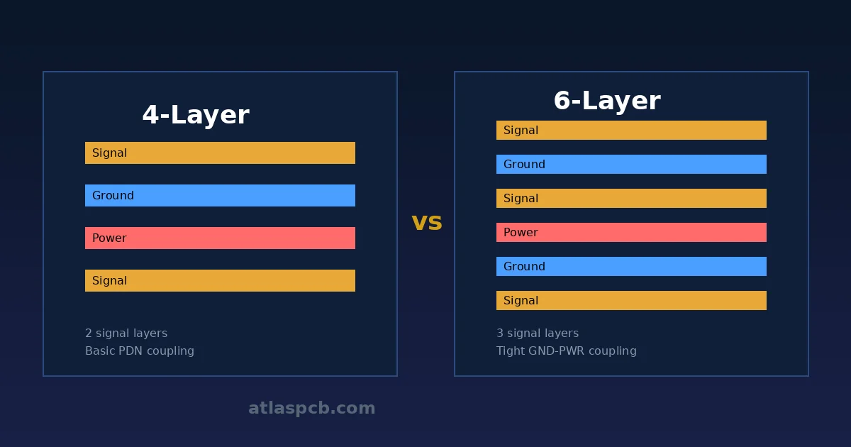
A 4-layer PCB adds two internal copper layers between the outer surfaces, separated by prepreg (partially cured fiberglass resin sheets) and laminated under heat and pressure. The standard stackup assigns these four layers with clear functional roles: the top layer carries signal traces and components, the first inner layer serves as a ground plane, the second inner layer serves as a power plane (or second ground plane in some configurations), and the bottom layer carries additional signal traces and components.
This structural difference is not merely about having “more room for routing.” The critical engineering advantage is that signals on the outer layers now sit directly adjacent to a continuous copper plane at a controlled, consistent distance. For a typical 4-layer stackup with standard prepreg, that distance is 10-12mil (0.25-0.30mm) between the outer signal layer and the adjacent ground plane. Compare this to a 2-layer board where the nearest ground reference might be 62mil (1.6mm) away on the opposite side of the board, or an inconsistent ground pour on the same layer at varying distances.
This geometry difference drives everything else discussed in this article: impedance control precision, EMI performance, power delivery quality, and manufacturing yield.
Signal Integrity and EMI: The Ground Plane Advantage
Every signal trace on a PCB has a return current that must flow back to the source. On a 2-layer board, that return current follows the path of least impedance through whatever ground copper is available — a pour, a trace, a via connection to the other side. At low frequencies (below a few MHz), the return current follows the path of least resistance, which might be a long, winding path through ground traces. At higher frequencies, the return current attempts to flow directly beneath the signal trace because this minimizes loop inductance.
The problem on 2-layer boards is that routing necessarily cuts through ground pours. Every signal trace routed across a ground pour on the same layer creates a gap that forces return current to detour around it. These detours create larger current loops, and larger loops radiate more electromagnetic energy. In our EMC pre-compliance measurements, we consistently see 10-15dB higher radiated emissions from 2-layer boards compared to equivalent 4-layer designs operating at the same clock frequencies.
On a 4-layer board with a solid inner ground plane, the return current flows directly underneath the signal trace on the adjacent plane layer with no interruptions (assuming you do not split the ground plane, which is a separate design error). The loop area formed by the signal trace and its return path is determined by the trace length multiplied by the dielectric thickness — typically just 10-12mil. This small loop area produces dramatically lower radiated emissions.
From a practical EMC perspective, we advise customers based on the following experience from our production: boards operating below 25MHz with relaxed EMC requirements (industrial environments, no FCC/CE testing) route successfully on 2 layers with careful ground pour management. Boards that must pass FCC Class B, CE, or any radiated emissions testing with signals above 50MHz almost always need a 4-layer stackup with unbroken ground planes. The engineering effort required to make a 2-layer board pass these tests at higher frequencies typically exceeds the cost difference of simply using four layers.
Impedance Control: Achievable Geometries on Each Stackup
Controlled impedance is where the structural difference between 2 and 4 layers becomes numerically concrete. Both can achieve impedance control, but the parameters are dramatically different.
On a standard 4-layer stackup with 1080 prepreg (dielectric thickness approximately 3.5mil after pressing, Dk approximately 4.2) between the signal layer and ground plane with 1oz copper, a 50-ohm microstrip requires a trace width of approximately 6.3mil. This is comfortable for most design rules and leaves abundant routing space. Differential pairs at 100-ohm impedance need approximately 5mil traces with 5mil spacing — well within standard manufacturing capabilities.
On a 2-layer board at 1.6mm thickness with 1oz copper, achieving 50-ohm microstrip referenced to a ground pour on the opposite side requires a trace width of approximately 70mil (1.78mm). This is impractical for high-density routing. The alternative is coplanar waveguide with ground (CPWG) geometry, where ground pours on the same layer flank the signal trace. With 4mil gaps to adjacent ground copper, approximately 12mil trace width achieves 50 ohms. This is workable but consumes lateral space and requires that the ground pour remains continuous and unbroken alongside every impedance-controlled trace.
The manufacturing tolerance is also significantly different. On a 4-layer board, impedance is controlled by the prepreg thickness, which is determined during lamination and is consistent across the entire board. Typical tolerance is plus or minus 10% of target impedance. On a 2-layer board using CPWG, impedance is controlled by the gap between the trace and adjacent ground pour, which depends on etching accuracy. Etching variation of plus or minus 0.5mil on a 4mil gap represents plus or minus 12.5% variation in the gap dimension, which translates to approximately plus or minus 5-8% impedance variation in best-case conditions but can be worse if the ground pour geometry is inconsistent.
For designs requiring differential impedance (USB, HDMI, Ethernet, PCIe), a 4-layer stackup is strongly preferred because the plane reference provides consistent impedance along the entire trace length rather than depending on ground pour continuity.
Power Delivery: Planes vs Pours
Power distribution quality is often overlooked in the 2-layer vs 4-layer discussion, but it affects every IC on the board through voltage droop and high-frequency noise on supply rails.
On a 2-layer board, power is distributed through traces and copper pours. A typical VCC pour might have an effective DC resistance of 5-15 milliohms depending on pour size and routing obstacles. More importantly, the inductance of a pour with traces routed through it can reach 2-5nH per centimeter of path length. When fast-switching digital ICs demand current transients (delta-I noise), this inductance causes voltage droops that scale with L times di/dt.
On a 4-layer board with a solid power plane, the DC resistance drops to below 1 milliohm for most practical board sizes, and the plane-to-plane capacitance between the ground and power layers provides inherent high-frequency decoupling. For a standard 4-layer stackup with 8mil dielectric between ground and power planes on a 100x100mm board, the interplane capacitance is approximately 500pF. While this seems small, it provides effective decoupling at frequencies above 500MHz where discrete capacitors become ineffective due to their mounting inductance.
The practical result: decoupling capacitors work significantly better on 4-layer boards because the loop from the capacitor pad through the via to the plane and back is just the via length (typically 1.2-1.6mm) rather than the potentially long trace path on a 2-layer board. We measure the effective decoupling frequency range extending 30-50% higher on 4-layer boards compared to equivalent capacitor placement on 2-layer designs.
For power-sensitive applications — precision ADCs, PLLs, RF synthesizers, or any circuit where power supply ripple translates directly to output noise — a 4-layer board with proper plane pairs is not optional. The improvement in supply rail quality is measurable and significant.
Interface-by-Interface Layer Count Guide
Rather than relying on vague frequency guidelines, here is a specific decision table based on common interfaces we see in production boards. These recommendations assume standard FR-4 material and typical board sizes (50x150mm range).
UART at baud rates below 1 Mbps works perfectly on 2-layer boards. The edge rates are slow enough that EMI is not a concern, and impedance matching is unnecessary. Even at 3 Mbps (common for GPS modules), 2 layers remain adequate.
I2C in standard mode (100 kHz) and fast mode (400 kHz) routes cleanly on 2 layers. Fast mode plus (1 MHz) is still acceptable on 2 layers with short traces. High-speed mode (3.4 MHz) benefits from a 4-layer board primarily for noise immunity rather than signal integrity.
SPI at clock rates below 10 MHz works reliably on 2-layer boards. Between 10-25 MHz, a 2-layer board works if trace lengths are kept under 5cm and ground return paths are unbroken. Above 25 MHz, or with trace lengths exceeding 10cm, a 4-layer board avoids clock integrity problems and reduces EMI.
CAN bus (1 Mbps or below) routes well on 2 layers because the differential signaling provides inherent noise rejection. CAN-FD at 5 Mbps still works on 2 layers with proper termination.
USB 2.0 Full Speed (12 Mbps) technically works on 2-layer boards for very short connections, but USB 2.0 High Speed (480 Mbps) requires a 4-layer board for impedance control of the 90-ohm differential pairs. USB 3.x and above absolutely require 4 or more layers.
100BASE-TX Ethernet (100 Mbps) is borderline — it can work on a well-designed 2-layer board with careful differential pair routing, but EMC certification becomes significantly more difficult. Gigabit Ethernet requires a 4-layer board without question.
DDR memory (any generation) requires 4 layers minimum, and DDR4/DDR5 typically require 6 or more layers for proper length matching and ground reference continuity across all data, address, and control groups.
HDMI, PCIe, SATA, and any multi-gigabit serial interface require 4 layers minimum with carefully controlled impedance stackups.
Real Production Cost Comparison
Cost comparisons in competitor articles tend to give single numbers without context. Here is our actual pricing data across three common board sizes, showing how the percentage premium changes with both board size and order quantity. All prices are for standard FR-4, 1.6mm thickness, 1oz copper, HASL finish, green solder mask, and standard lead times.
For a small board at 50x50mm (typical for a sensor module or simple controller), 5-piece prototype pricing runs approximately 8-12 USD total for 2-layer and 18-25 USD for 4-layer — roughly a 100-120% premium driven by the fixed lamination setup cost that cannot be amortized. At 100 pieces, the cost is approximately 0.45-0.60 USD per board for 2-layer and 0.70-0.95 per board for 4-layer, bringing the premium down to approximately 55-60%. At 1000 pieces, per-unit costs converge further to 0.25-0.35 for 2-layer and 0.35-0.50 for 4-layer, a premium of approximately 40%.
For a medium board at 100x100mm (typical for a main controller board or IoT gateway), prototype pricing is approximately 15-20 USD total for 2-layer and 30-40 USD for 4-layer — about 80-100% premium. At 100 pieces, per-board cost is approximately 1.20-1.60 for 2-layer and 1.80-2.40 for 4-layer (50-55% premium). At 1000 pieces, 0.70-0.90 for 2-layer and 0.95-1.25 for 4-layer (35-40% premium).
For a larger board at 150x100mm (typical for a communication or industrial control board), prototype pricing is approximately 25-35 USD total for 2-layer and 45-60 USD for 4-layer (75-85% premium). At 100 pieces, 2.00-2.60 per board for 2-layer and 2.90-3.80 for 4-layer (45-50% premium). At 1000 pieces, 1.10-1.50 for 2-layer and 1.50-2.00 for 4-layer (35-40% premium).
The pattern is clear: the percentage premium decreases as volume increases because the fixed costs of inner-layer processing and lamination become a smaller fraction of total cost. At production volumes, the cost difference between 2 and 4 layers is rarely the deciding factor — it is a 30-40% premium on the bare board, which is typically a small fraction of the total assembled BOM cost.
Get an Instant Layer Count Recommendation
Upload your Gerber files or schematic for a free DFM review. Our engineers will recommend the optimal layer count for your specific design with actual cost quotes for both options.
Request DFM ReviewLead Time and Manufacturing Process Differences
A 2-layer PCB follows a straightforward manufacturing flow: drill, plate through holes, apply photoresist, expose and develop outer layer pattern, etch, strip resist, apply solder mask, screen legend, surface finish, profile routing, and electrical test. Total processing time is typically 3-5 business days for standard orders.
A 4-layer PCB inserts several additional steps before the outer layer processing begins. The inner layers (ground and power planes) are imaged, etched, and inspected independently using automated optical inspection (AOI). This inner-layer inspection is critical because defects on inner layers cannot be repaired after lamination. The inspected inner layers are then oxidized (brown or black oxide treatment for adhesion), stacked with prepreg sheets, and laminated in a hydraulic press at temperatures around 180 degrees Celsius and pressures of 250-400 PSI for 60-90 minutes. After lamination, the panel is drilled through all layers, and the remaining outer-layer processing follows the same sequence as a 2-layer board. Total processing time is typically 5-7 business days.
From a DFM perspective, each approach has specific failure modes that designers should understand. On 2-layer boards, the most common manufacturing issues we encounter are copper balance problems causing board warpage (particularly on boards thinner than 1.0mm), ground pour islands that create acid traps during etching, and insufficient annular ring around vias where dense routing passes between pads. On 4-layer boards, the most common issues are inner-layer registration errors (particularly on larger panels where thermal expansion during lamination causes layer shift), lamination voids from trapped moisture or contamination between prepreg layers, and misalignment between inner-layer pads and drilled holes when aspect ratios are high.
Both sets of issues are manageable with proper design rules and DFM review, but they represent different categories of risk that your manufacturer should check before production.
Migration Guide: Upgrading a 2-Layer Design to 4 Layers
If you have an existing 2-layer design that has outgrown its layer count — perhaps it failed EMC testing, or you need to add a higher-speed interface in a revision — upgrading to 4 layers does not necessarily require a complete redesign. Here is the practical migration path we recommend to customers in this situation.
First, preserve your component placement. In most cases, the physical layout of components is driven by mechanical constraints, thermal considerations, and user interface requirements that do not change with layer count. Keep what works.
Second, define your new stackup. The most common migration target is signal-ground-power-signal with standard 1080 prepreg (approximately 3.5mil) between each signal layer and its adjacent plane. This means your signal-to-reference distance changes from 62mil (half of 1.6mm board thickness) to approximately 3.5-5mil. Every trace width must be recalculated for the new geometry.
Third, move your ground pours to a solid inner ground plane. Convert all ground pour polygons on both outer layers into via connections to the inner ground plane. Place ground vias at a density of at least one via per 200mil spacing in critical areas. This step alone delivers most of the EMI improvement.
Fourth, establish your power distribution on the second inner plane. Route VCC, 3.3V, 5V, and any other power rails as zones on this inner layer rather than traces on the outer layers. This frees significant routing space on the outer layers.
Fifth, recalculate trace widths for the new impedance geometry. Your 50-ohm traces will be much narrower — approximately 6mil instead of 12-70mil depending on your previous geometry. This is actually an advantage because narrower traces provide more routing space.
Sixth, perform a new DFM check. The design rules for a 4-layer board are slightly different: minimum via-to-plane clearance (typically 8mil), inner-layer copper-to-board-edge clearance (minimum 20mil), and registration tolerance allowances for inner-layer features.
Most designs complete this migration in one to two engineering days rather than a full redesign cycle, because the signal topology and component relationships remain unchanged.
Need Help with a Layer Count Upgrade?
If your 2-layer board is struggling with EMC or signal integrity, our engineering team can review your design and recommend the most cost-effective migration path to 4 layers.
Submit Design for ReviewThe 5-Question Decision Checklist
After processing thousands of customer designs across both layer counts, we have distilled the decision to five concrete questions. Answer yes to any of the first four, and a 4-layer board is the engineering-correct choice.
Does your design include any signal with an edge rate faster than 5 nanoseconds or a clock frequency above 50 MHz? If yes, those signals need a continuous reference plane within 5-12mil to maintain signal integrity and control EMI. A 4-layer board provides this inherently.
Does your BOM include any BGA package or QFP/QFN with pitch below 0.5mm? If yes, escape routing from these packages typically requires the additional routing freedom that inner planes provide on the outer layers. Forcing escape routes through narrow channels on a 2-layer board compromises ground continuity.
Must your product pass FCC Class B, CE, or equivalent radiated emissions testing? If yes, and your design includes digital logic operating above 25 MHz, the EMI margin provided by solid ground planes will likely save you at least one re-test cycle. Budget the 4-layer premium into your bill of materials rather than risking a failed certification.
Is your board area constrained to less than 50x50mm while carrying more than 30 components? If yes, the routing density on two layers will almost certainly fragment ground pours to the point where they provide minimal return-current benefit. Four layers give you back that ground integrity.
If you answered no to all four questions above, a 2-layer board is appropriate. Your design is simple enough, slow enough, and spacious enough that two well-managed copper layers provide adequate performance at lower cost.
Thermal Considerations: A Factor Most Guides Miss
Layer count also affects thermal management, though this is rarely discussed in comparison articles. Copper planes are excellent lateral heat spreaders. On a 4-layer board, the internal ground and power planes act as thermal spreading layers that distribute heat from hot components (voltage regulators, power transistors, processors) across a larger board area, reducing peak temperatures.
On a 2-layer board, heat spreading is limited to the copper pours on top and bottom layers, which are typically fragmented by routing. Thermal vias from a component’s thermal pad connect only to copper on the opposite side, and the path resistance depends on pour continuity.
In our thermal testing of power regulator circuits, we have measured a consistent 8-15 degree Celsius reduction in peak component temperature when the same design is implemented on a 4-layer board versus a 2-layer board, with identical copper area on the outer layers. The difference is entirely attributable to the lateral heat spreading through internal planes.
For designs with components dissipating more than 1-2 watts in a confined area, the thermal improvement from internal planes can be the deciding factor for layer count selection independent of any electrical signal considerations.
Compare Your Options with Real Pricing
Upload your design files and receive quotes for both 2-layer and 4-layer configurations within 24 hours. No obligation, no sales pressure — just the data you need to make the right engineering decision.
Get Comparative QuotesMaking the Final Decision
The layer count decision is ultimately about engineering margin versus cost. A 2-layer board works when the margin is naturally present — low frequencies, generous board area, relaxed EMC requirements, and simple routing topology. A 4-layer board becomes necessary when the design needs controlled margins — precise impedance, predictable return currents, certified EMC performance, and dense routing without compromise.
The cost premium of 30-50% on the bare board is real, but context matters. In a typical assembled board with a BOM cost of 15-50 USD, the bare board represents 5-15% of total assembly cost. The layer count premium is therefore 2-7% of the total assembled unit cost — a fraction that is almost always justified if it prevents a single EMC re-test, one assembly rework cycle, or a board spin that delays your product launch by weeks.
Our recommendation is straightforward: if you are uncertain, start with four layers. The engineering headroom costs less than you think, and it eliminates an entire category of problems that are expensive to diagnose and fix after the fact. Reserve 2-layer boards for designs where simplicity is genuinely appropriate and the cost difference at your production volume makes a meaningful impact on unit economics.
Reviewed by AtlasPCB Engineering Team. Technical specifications reflect our standard manufacturing capabilities on FR-4 material as of August 2026.
About AtlasPCB — We specialize in complex PCB manufacturing for HDI, RF, and high-reliability applications. Explore our impedance-controlled PCB manufacturing, or get an free engineering DFM review . Every order includes free engineering review. Get your quote.
Reviewed by AtlasPCB Engineering Team — IPC-certified manufacturing specialists with 15+ years of production experience in HDI, RF, and high-reliability PCB fabrication. Content based on factory floor data and real customer design reviews.
Frequently Asked Questions
How much more expensive is a 4-layer PCB than a 2-layer?
Can you do impedance control on a 2-layer PCB?
At what frequency should I switch from 2-layer to 4-layer?
Does a 4-layer PCB take longer to manufacture?
Can I upgrade my 2-layer design to 4 layers without a complete redesign?
- 2 layer PCB
- 4 layer PCB
- PCB stackup
- PCB design
- multilayer PCB
- impedance control
- EMI
- PCB cost
- DFM
- PCB layer count