· AtlasPCB Engineering · Engineering · 9 min read
Impedance Controlled PCB: DFM Specification Guide for Your First Order
How to specify impedance controlled PCBs correctly — trace geometry, stackup callouts, coupon requirements, and the DFM mistakes that cause impedance failures. Based on 500+ production orders.
Quick Answer
To specify impedance controlled PCBs: define target impedance (+/-10% or +/-5%), specify reference layer for each controlled trace, provide stackup with dielectric thickness and Dk values, call out TDR coupon testing, and maintain minimum 3x dielectric height clearance to adjacent traces. Most first-order failures come from missing reference plane callouts or unrealistic tolerance on FR-4.
Quick Answer: Impedance Specification Checklist
Before submitting your design for impedance controlled fabrication, confirm these six items are documented in your fab drawing or stackup notes:
| Item | What to Specify | Common Mistake |
|---|---|---|
| Target impedance | ”50 ohm +/-10%” or “90 ohm diff +/-5%“ | Specifying impedance without tolerance |
| Reference layer | ”L1 signals referenced to L2 ground” | Not identifying which plane is reference |
| Controlled layers | ”L1, L3, L6 require impedance control” | Marking all layers as controlled (costly) |
| Material Dk | ”FR-4, Dk 4.2 at 1 GHz” or “Rogers 4350B” | Assuming Dk without specifying frequency |
| TDR coupons | ”TDR verification required, report with shipment” | Not requesting measurement proof |
| Trace geometry | Single-ended width or diff pair width/space | Hard-coding widths that conflict with target Z |
If any of these are missing from your documentation, your manufacturer is guessing — and guessing is how you get boards that measure 42 ohms instead of 50.
What Impedance Control Actually Means in Fabrication
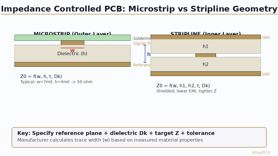
Impedance control is not a special process bolted onto standard PCB manufacturing — it is a tightening of the same process variables that always exist. Every PCB trace has a characteristic impedance determined by its width, copper thickness, dielectric height to the reference plane, and the dielectric constant of the material between them. When you specify “impedance controlled,” you are telling the manufacturer to actively manage these variables within defined limits and prove the result with measurement.
In practice, this means the manufacturer runs your stackup through a 2D field solver (typically Polar Si9000 or equivalent), calculates the trace widths needed to hit your target impedances on their actual material (using their measured Dk values from incoming inspection, not datasheet nominals), and then controls etch to hold those trace widths within a process window that keeps impedance within your specified tolerance.
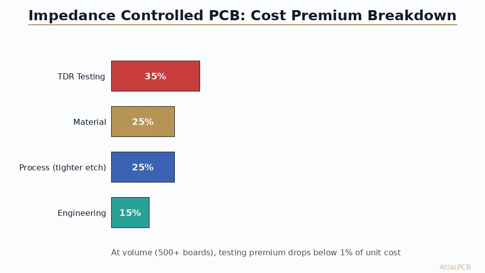
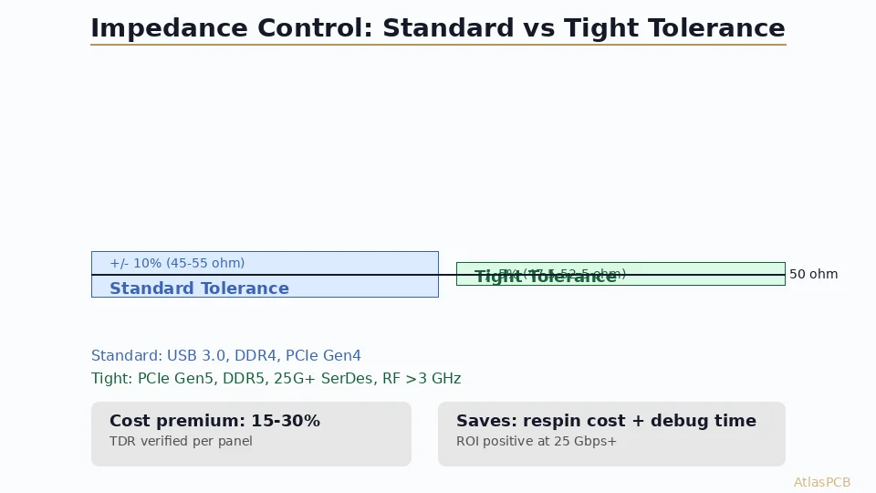
The common misconception is that impedance control means exotic processing. It does not. It means controlled processing — tighter etch windows, verified material properties, and coupon measurement to prove conformance. This is why impedance control adds 15-30% to board cost: not because the process is different, but because the tolerance band is narrower and verification (TDR testing) is mandatory.
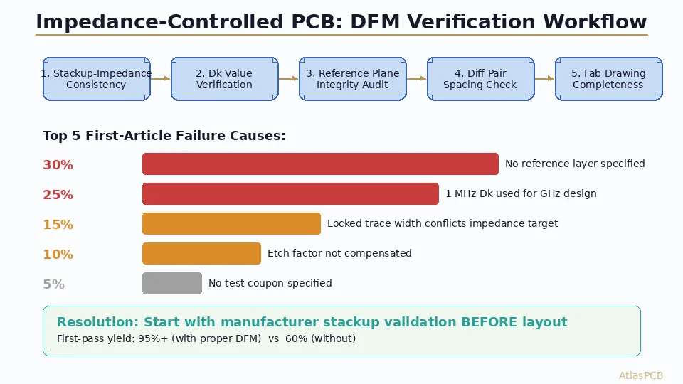
Based on our production data across 500+ impedance-controlled orders this year, the most frequent reasons for impedance failure are (in order): incorrect Dk assumption in the customer’s simulation, etch variation exceeding the process window, and prepreg resin flow during lamination shifting actual dielectric thickness from nominal. Understanding these failure modes helps you specify correctly.
IMPEDANCE CONTROLLED PCB MANUFACTURER
TDR-Verified Impedance on Every Lot
We model your stackup before production, fabricate with measured Dk values, and ship with TDR coupon reports. Single-ended and differential, +/-5% on Rogers, +/-7% on FR-4.
Upload Gerbers for Impedance Review ›
DFM Mistakes That Cause Impedance Failures
After reviewing thousands of designs submitted for impedance-controlled fabrication, our process engineering team has identified the failure patterns that recur most frequently. These are the issues we catch in DFM review that, if missed, result in boards that fail TDR verification.
Mistake 1: Wrong Dk Value in Simulation
The single most common error. Engineers simulate their stackup using a generic “FR-4 Dk = 4.5” value pulled from a textbook, then wonder why fabricated boards measure 10% off target. Real Dk depends on resin content, glass style, frequency, and the specific laminate product. Isola 370HR at 50% resin content has a Dk of approximately 3.9 at 1 GHz — not 4.5. If you simulated at 4.5 and we fabricate at 3.9, your 50-ohm trace will measure 56 ohms.
The fix: ask your manufacturer what Dk value they use for impedance modeling on their specific material. We publish our measured Dk values for every laminate we stock, and our field solver uses these measured values — not datasheet figures.
Mistake 2: Missing or Wrong Reference Plane Identification
Impedance is defined between a signal trace and its reference plane. On a 6-layer board, L1 signals might reference L2 (ground) or L3 (power) — the impedance is dramatically different because dielectric thickness changes by 2-3x. If your fab drawing does not explicitly state which plane each signal layer references, the manufacturer has to guess, and they may guess differently than your simulator.
A common failure mode we see: an engineer designs differential pairs on L1 referenced to L2 ground, but the manufacturer interprets L1 as referenced to L3 (a thicker dielectric) and calculates wider traces. The traces etch correctly for L3 reference — but the actual impedance measured against L2 is 15% too low.
Mistake 3: Soldermask Effect Ignored
Soldermask has a Dk of approximately 3.3-3.8 depending on formulation and thickness. On outer-layer microstrip traces, soldermask covering the trace lowers impedance by 2-5 ohms compared to an exposed trace. For designs at +/-10% tolerance this usually stays within spec. For +/-5% tolerance, soldermask effect must be included in the impedance model.
If your simulation assumes bare copper (no soldermask), specify soldermask opening over impedance-controlled traces — or accept that the actual impedance will be 2-5 ohms lower than simulated. Our field solver includes soldermask effect in all outer-layer calculations by default.
Mistake 4: Copper Plating Thickness Not Accounted For
Base copper on inner layers is typically 0.5 oz (17.5 um) or 1 oz (35 um) — what you specified. But outer layers receive additional copper during electroless deposition and electroplating, typically adding 20-25 um on top of the base copper. This extra copper height changes the trace cross-section geometry and affects impedance. Our solver accounts for actual plated thickness, but if you simulated with only base copper, there will be a discrepancy.
PCB DFM CHECK
Catch These Issues Before Fabrication
Our DFM review catches impedance specification errors, reference plane conflicts, and stackup issues before they become failed boards. Submit your design for engineering review.
Stackup Design for Impedance: Practical Guidelines
The stackup is where impedance control succeeds or fails. A well-designed stackup makes impedance achievable with standard process tolerances. A poorly designed one makes even tight process control insufficient.
The fundamental rule: thinner dielectric gives you more impedance control authority. With a 4-mil (100 um) core between signal and reference plane, a 1-mil change in trace width shifts impedance by approximately 5 ohms. With an 8-mil core, the same 1-mil width change shifts impedance by only 3 ohms. The thinner dielectric means the trace geometry dominates over other variables, giving the process more margin.
However, there are practical limits. Below 3 mils (75 um) dielectric thickness, the layer-to-layer registration and prepreg flow variation during lamination become significant relative to the total thickness. For reliable +/-5% impedance on production panels, we recommend minimum 3.5 mil dielectric for outer-layer microstrip and minimum 4 mil for inner-layer stripline.
For differential pairs, the spacing between the two traces is equally important as the trace width. Tightly coupled pairs (space less than 2x dielectric height) have strong mutual coupling that affects impedance. Loosely coupled pairs (space greater than 3x dielectric height) behave essentially as two independent single-ended traces. Most high-speed interfaces (USB 3.x, PCIe Gen 4/5, HDMI 2.1) specify 100-ohm differential impedance with moderate coupling — we typically target trace width of 4-5 mil with 5-6 mil space on inner layers with 4 mil dielectric.
For designs requiring both 50-ohm single-ended and 100-ohm differential on the same layer referenced to the same plane, the math works out cleanly: the differential pair trace width will be narrower than the single-ended trace width. This is normal and expected — do not force both to the same width.
Our PCB stackup design guide covers layer assignment strategy in detail for 4-, 6-, 8-, and 10-layer boards with impedance requirements.
How to Specify: The Fab Drawing Template
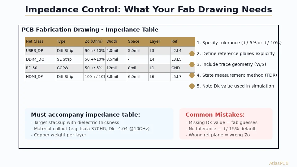
The cleanest way to communicate impedance requirements is a dedicated impedance table in your fab drawing or separate impedance specification document. Here is the format our engineering team processes most efficiently:
Impedance Control Table:
| Net Class | Type | Target Z | Tolerance | Layer | Reference | Notes |
|---|---|---|---|---|---|---|
| USB3_DP/DN | Differential | 90 ohm | +/-10% | L1 | L2 (GND) | Include soldermask effect |
| PCIE_TX/RX | Differential | 100 ohm | +/-10% | L3 | L2, L4 (GND) | Stripline, symmetric |
| RF_OUT | Single-ended | 50 ohm | +/-5% | L1 | L2 (GND) | Rogers 4350B, exposed (no mask) |
| CLK_100M | Single-ended | 50 ohm | +/-10% | L3 | L2, L4 | FR-4 stripline |
Also specify in the stackup section:
- Material: “FR-4, Isola 370HR or equivalent, Dk 4.0 +/-0.1 at 1 GHz”
- Prepreg: “1080, 2x 2116, or equivalent to achieve stated dielectric thickness”
- Finished copper: “1 oz outer (with plating), 0.5 oz inner”
- Tolerance note: “Trace widths may be adjusted by manufacturer to meet impedance targets”
That last note is critical. It gives the manufacturer permission to modify trace widths from your CAD output to hit impedance targets based on their actual material Dk. Without this permission, some manufacturers fabricate your exact CAD trace widths even if they know the resulting impedance will miss spec — because you did not authorize adjustment.
ATLASPCB
Submit Your Impedance-Controlled Design
Upload Gerbers with your impedance table. We model your stackup on our actual materials, confirm trace widths, and return a quote with impedance simulation results — before production starts.
Get Impedance Quote ›
Reviewed by AtlasPCB Engineering Team — 15+ years in advanced PCB fabrication for RF, HDI, and rigid-flex applications.
Related Reading:
About AtlasPCB — We specialize in complex PCB manufacturing for HDI, RF, and high-reliability applications. Explore our impedance-controlled PCB manufacturing, or get an free engineering DFM review . Every order includes free engineering review. Get your quote.
Reviewed by AtlasPCB Engineering Team — IPC-certified manufacturing specialists with 15+ years of production experience in HDI, RF, and high-reliability PCB fabrication. Content based on factory floor data and real customer design reviews.
Frequently Asked Questions
What tolerance should I specify for impedance controlled PCB?
Do I need impedance control on all traces?
What is a TDR coupon and do I need one?
How does trace width affect impedance?
What information must I provide to my PCB manufacturer for impedance control?
- impedance controlled PCB manufacturer
- PCB DFM check
- PCB stackup design guide
- controlled impedance
- signal integrity