· AtlasPCB Engineering · Engineering · 9 min read
5G FWA/CPE Router PCB Design: Rogers 4350B Hybrid Stackup for Sub-6 GHz and mmWave Bands
Fixed wireless access (FWA) customer premises equipment requires dual-band PCB designs supporting both sub-6 GHz (n77/n78) and mmWave (n258/n260/n261) simultaneously. This guide covers the Rogers-FR4 hybrid stackup that delivers RF performance on antenna layers while keeping digital section costs manageable for volume CPE production.
Quick Answer
5G FWA/CPE router PCBs use a Rogers-FR4 hybrid stackup to optimize cost and RF performance simultaneously. The antenna layers (top and bottom) use Rogers RO4350B (Dk 3.66, Df 0.0037) for low-loss patch antenna elements and feed networks, while the inner layers use standard high-Tg FR-4 for digital baseband, power distribution, and Ethernet routing. This hybrid approach saves 40-60% versus full Rogers construction while achieving equivalent antenna gain and radiation efficiency at both sub-6 GHz and mmWave frequencies.
The Design Challenge: Two Radios, One PCB
Fixed wireless access CPE hardware faces a unique PCB design challenge: the device must integrate antenna arrays for two vastly different frequency ranges — sub-6 GHz (typically n77/n78 at 3.3-3.8 GHz) and optionally mmWave (n258 at 24.25-27.5 GHz or n260 at 37-40 GHz) — on a single PCB that also carries all digital baseband processing, power management, Ethernet switching, and WiFi connectivity.
The sub-6 GHz antennas are physically large (patch elements approximately 25x25mm at 3.5 GHz) but relatively tolerant of substrate loss. The mmWave antennas are tiny (patch elements approximately 3x3mm at 28 GHz) but extremely sensitive to both substrate loss and dimensional tolerance. Meanwhile, the digital section needs dense routing for DDR4/DDR5 memory interfaces, PCIe lanes to the 5G modem, and Gigabit Ethernet — none of which requires exotic substrate material.
The economic reality for FWA CPE is harsh: these devices ship in volumes of 100,000 to millions of units, and retail pricing targets $200-600. Every dollar of PCB cost matters at scale. Using full Rogers construction would add $15-30/board at volume — potentially $2-5M in material cost for a million-unit production run. The hybrid stackup solves this by applying Rogers only where RF physics demands it.
Recommended 8-Layer Hybrid Stackup
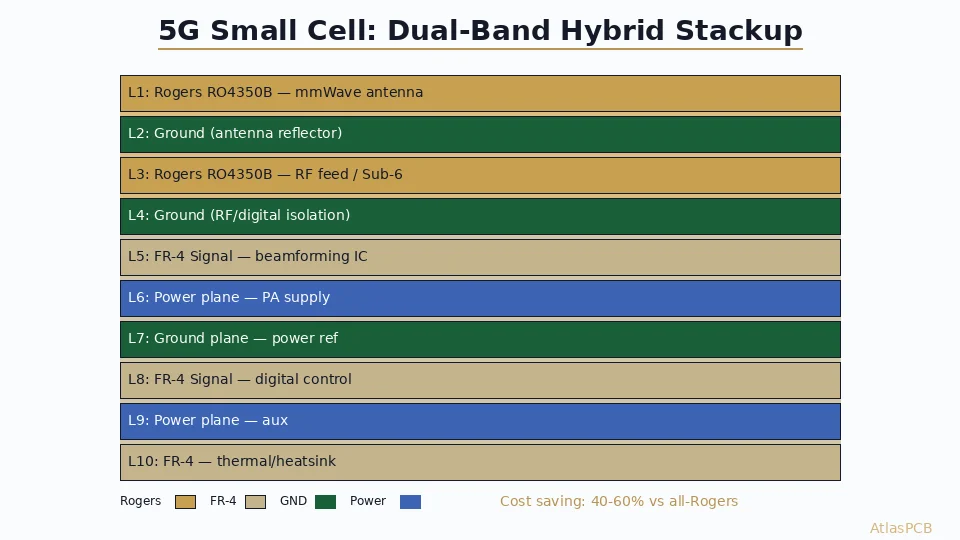
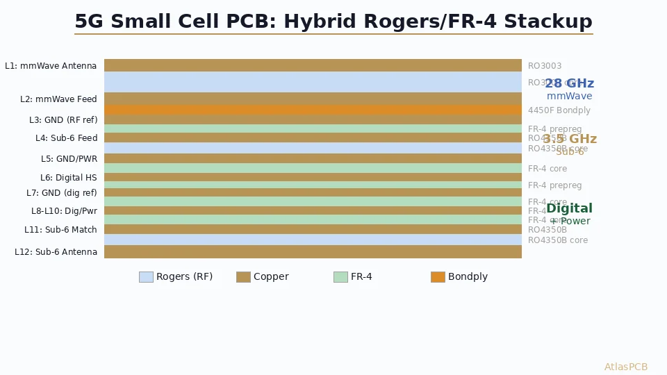
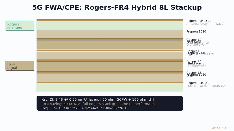
The following stackup has been validated across multiple 5G FWA CPE programs in production. It supports dual-band operation (sub-6 + mmWave) with adequate layer count for digital routing complexity.
| Layer | Material | Thickness | Function | Dk/Df |
|---|---|---|---|---|
| L1 (Top) | Rogers RO4350B | 0.168mm (6.6 mil) | mmWave antenna array | 3.66/0.0037 |
| Bondply 1 | Rogers 4450F | 0.100mm (4 mil) | Rogers-to-copper bonding | 3.52/0.004 |
| L2 | Copper 1oz | 35um | GND reference (mmWave) | — |
| Core 1 | FR-4 High-Tg 170 | 0.200mm (8 mil) | — | 4.2/0.018 |
| L3 | Copper 1oz | 35um | Digital signal (PCIe, DDR) | — |
| Prepreg | FR-4 2116 | 0.120mm | Bonding | 4.2/0.018 |
| L4 | Copper 1oz | 35um | Power plane | — |
| Core 2 | FR-4 High-Tg 170 | 0.200mm (8 mil) | — | 4.2/0.018 |
| L5 | Copper 1oz | 35um | Power/GND split | — |
| Prepreg | FR-4 2116 | 0.120mm | Bonding | 4.2/0.018 |
| L6 | Copper 1oz | 35um | Digital signal (Ethernet, WiFi) | — |
| Core 3 | FR-4 High-Tg 170 | 0.200mm (8 mil) | — | 4.2/0.018 |
| L7 | Copper 1oz | 35um | GND reference (sub-6 GHz) | — |
| Bondply 2 | Rogers 4450F | 0.100mm (4 mil) | Rogers-to-copper bonding | 3.52/0.004 |
| L8 (Bottom) | Rogers RO4350B | 0.254mm (10 mil) | Sub-6 GHz antenna + feed | 3.66/0.0037 |
Total board thickness: approximately 1.8-2.0mm (within standard PCB thickness range)
The asymmetry between L1 (6.6 mil Rogers) and L8 (10 mil Rogers) reflects the different antenna requirements: mmWave patches on thin substrate for wider bandwidth, sub-6 GHz patches on thicker substrate for higher gain. The ground planes on L2 and L7 provide clean RF reference and isolation between the antenna sections and the digital core.
5G RF PCB MANUFACTURING
Rogers-FR4 Hybrid for 5G FWA
Production-qualified Rogers RO4350B hybrid processing. Antenna impedance verification and radiation pattern correlation available.
Get RF PCB Quote ›
Critical Design Rules for 5G FWA Router PCBs
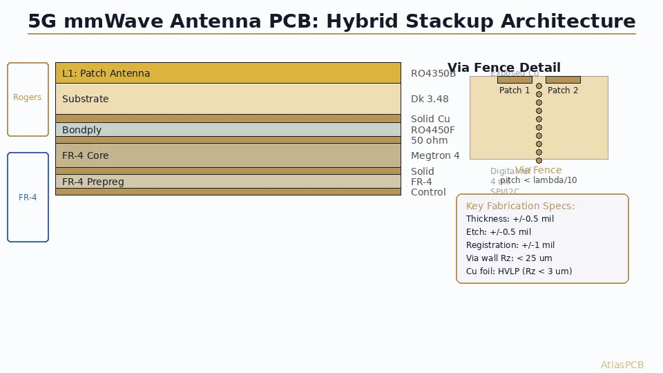
Antenna element tolerance: At mmWave frequencies, patch antenna dimensions must be controlled to +/-25um (1 mil) for center frequency accuracy within +/-100 MHz. Standard PCB etching with +/-50um (2 mil) tolerance shifts the antenna resonance by 200-400 MHz at 28 GHz — often outside the operating band. Specify tight etch tolerance on L1 antenna elements, with measurement verification against a known-good reference.
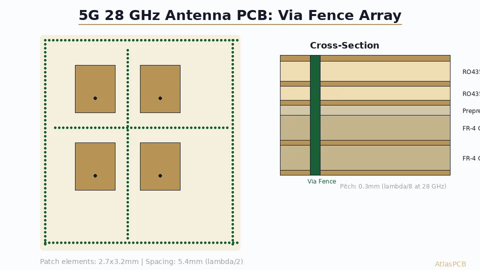
Via fencing around mmWave feed networks: The grounded coplanar waveguide (GCPW) feed network on L1 requires via fencing with pitch no greater than lambda/10 at the operating frequency. At 28 GHz (lambda = 10.7mm in air, approximately 5.6mm in RO4350B), via pitch must be 0.56mm or less. This creates dense via arrays surrounding every mmWave trace — ensure your manufacturer can achieve 0.25mm drill at 0.56mm pitch without via-to-via copper bridging.
Transition between Rogers and FR-4 layers: Signal vias passing through the Rogers-FR4 bondply interface see a Dk discontinuity (3.52 to 4.2). For the digital signals routed on inner layers, this is negligible. But for any RF signal that must transition between layers (e.g., mmWave feed connecting to a balun or LNA on L3), the via structure must be impedance-matched with appropriate anti-pad sizing and ground via cage.
Thermal management: 5G modems (Qualcomm SDX65/SDX75, MediaTek T750) dissipate 3-8W of thermal power. The FR-4 core layers between L3-L6 provide adequate thermal conductivity for heat spreading when combined with thermal vias under the modem package. Do not place thermal vias through the Rogers layers — drill damage to Rogers material during thermal via formation can create delamination points at the bondply interface.
Manufacturing Process Considerations
Fabricating Rogers-FR4 hybrid boards requires specific process knowledge that not every PCB manufacturer possesses. The critical process steps where failures occur:
Rogers surface preparation: RO4350B requires plasma treatment or sodium-naphthalene etch for proper adhesion to the bondply. Standard FR-4 oxide treatments (brown/black oxide) do not create adequate adhesion to Rogers ceramic-filled hydrocarbon substrate. Manufacturers without Rogers experience frequently skip this step, resulting in delamination during thermal stress (reflow soldering or thermal cycling).
Bondply lamination profile: Rogers 4450F bondply requires a specific lamination temperature profile: 30-minute ramp to 220C, 60-minute hold at 220C, 400 psi pressure. This differs significantly from standard FR-4 lamination (175-180C, 250-300 psi). Shops running mixed Rogers/FR-4 layups must use the Rogers profile — if they default to FR-4 parameters, the bondply does not fully cure, creating weak adhesion that appears fine initially but fails under thermal cycling.
Drilling through Rogers + FR-4: Standard carbide drill bits work for both materials, but entry/exit conditions differ. Rogers material tends to produce cleaner holes with less smear, while FR-4 requires proper backup material to prevent exit burr. The hybrid stackup presents the drill with alternating material types — experienced fabricators adjust feed rate at the material transitions to prevent delamination at the Rogers-bondply-copper interface.
In our production environment, we maintain separate Rogers-qualified lamination programs and drill parameter sets specifically for hybrid constructions. Panel-level Rogers adhesion verification (peel strength testing per IPC-TM-650 2.4.8) runs on every production lot to catch process drift before it reaches your boards.
ROGERS PROCESSING EXPERTISE
Production-Qualified Hybrid Stackup Processing
Validated Rogers 4450F bondply lamination, plasma surface treatment, and panel-level adhesion testing on every lot. Not a standard FR-4 shop attempting Rogers.
Cost Optimization for Volume FWA Production
At CPE production volumes (10,000-100,000+ units), every design decision that affects PCB cost multiplies across the entire production run. The following optimization strategies reduce hybrid stackup cost by 15-30% without sacrificing RF performance:
Use RO4350B instead of RO4835 for sub-6 GHz layers. At 3.5 GHz, the Df difference between RO4350B (0.0037) and RO4835 (0.0037) is negligible. RO4350B is more widely stocked and available in more thickness options, reducing material lead time and cost. Reserve RO4835 or RO3003 only if your design operates above 30 GHz where every 0.001 Df matters.
Minimize Rogers panel area. If your antenna elements only occupy 40% of the board area on L1, consider a selective Rogers approach: Rogers material only under the antenna array, with FR-4 on the remainder. This “island” construction reduces Rogers material consumption by 50-60% per panel. However, it adds process complexity (selective lamination), so it only makes economic sense above 5000 units where the material savings exceeds the NRE and process premium.
Panel utilization optimization. Rogers material comes in standard sheet sizes (18x24”, 18x12”). Work with your manufacturer to optimize the panel array (number of boards per panel) to minimize Rogers material waste. A 120x80mm FWA router board fits 4-up on a standard 18x24” panel with good utilization, but an oddly-shaped design might only fit 2-up with 30% waste.
Combine orders across product variants. If you manufacture multiple FWA CPE variants (indoor unit, outdoor unit, enterprise unit), standardize the stackup construction across variants. Using the same Rogers thickness, bondply, and FR-4 core across all products allows your manufacturer to batch material procurement — securing 10-15% volume discount on Rogers material that passes through to your pricing.
Antenna Performance Verification
The most important PCB-level qualification for 5G FWA boards is antenna performance correlation: comparing measured antenna gain, bandwidth, and radiation pattern against simulation predictions. Discrepancies reveal either fabrication issues (dimensional errors, material property deviation) or design issues (inadequate ground plane, coupling to nearby structures).
For sub-6 GHz antennas, expect measured gain within +/-0.5 dB of simulation and bandwidth within +/-50 MHz when fabrication is properly controlled. For mmWave arrays, tighter correlation (+/-0.3 dB, +/-30 MHz) is achievable with tight etch control but requires specific measurement setup (far-field range or near-field scanner).
Our engineering team supports antenna correlation by providing measured Dk/Df values from production panel test coupons. This data feeds back into your electromagnetic simulation for more accurate prediction of antenna performance before committing to production, reducing the typical 2-3 antenna tuning iterations to 1-2.
ATLASPCB
5G Antenna PCB Manufacturing at Volume
Rogers-FR4 hybrid stackup, production-qualified process, Dk/Df coupon data for antenna correlation. Supporting 5G FWA/CPE programs from prototype through mass production.
Get Volume Pricing ›
Reviewed by AtlasPCB Engineering Team — 15+ years in advanced PCB fabrication for RF, HDI, and rigid-flex applications.
Related Reading:
About AtlasPCB — We specialize in complex PCB manufacturing for HDI, RF, and high-reliability applications. Explore our RF and high-frequency PCB services, Rogers RO4350B PCB manufacturing, or get an multilayer PCB fabrication up to 30 layers . Every order includes free engineering review. Get your quote.
Reviewed by AtlasPCB Engineering Team — IPC-certified manufacturing specialists with 15+ years of production experience in HDI, RF, and high-reliability PCB fabrication. Content based on factory floor data and real customer design reviews.
Frequently Asked Questions
Why do 5G FWA routers need Rogers material?
How much does a 5G FWA router PCB cost with Rogers layers?
What stackup works for dual-band 5G FWA (sub-6 + mmWave)?
Can Chinese PCB manufacturers produce 5G FWA router boards?
What impedance control is needed for 5G FWA antenna feeds?
- 5G antenna PCB fabrication
- Rogers 4350B stackup
- RF PCB design and manufacturing
- 5G CPE
- China RF PCB manufacturer