· AtlasPCB Engineering · Engineering · 11 min read
5G Antenna PCB Fabrication for Indoor mmWave Repeaters: Material, Stackup, and Manufacturing Challenges at 24-28 GHz
Technical manufacturing guide for 5G indoor mmWave repeater PCBs operating at 24-28 GHz (n257/n258/n261 bands). Covers Rogers material selection, hybrid stackup design, antenna-in-package PCB requirements, via fencing for isolation, and the specific fabrication tolerances that determine whether your repeater design meets 3GPP EVM specifications in production.
Quick Answer
5G indoor mmWave repeater PCBs at 24-28 GHz require Rogers 4350B or equivalent low-loss laminate on antenna and RF front-end layers, with FR-4 acceptable for digital baseband and power distribution. Critical fabrication tolerances include: copper etching at +/-0.5mil for 50-ohm GCPW traces (typically 8-10mil wide on 5mil Rogers), via fencing pitch at lambda/10 or tighter (approximately 0.4mm at 28 GHz), and surface roughness below Rz 3um on RF copper to limit conductor loss below 0.5 dB/cm. Panel-to-panel Dk consistency of +/-0.02 (achievable with Rogers, not with FR-4) is essential for repeater designs where antenna elements must maintain calibrated phase across production units.
Quick Reference: 5G Indoor mmWave Repeater PCB Specifications
| Parameter | Requirement at 24-28 GHz | Why It Matters |
|---|---|---|
| RF layer material | Rogers RO4350B or RO4003C | Df < 0.005 at 28 GHz required |
| Copper roughness (RF layers) | VLP/HVLP (Rz < 3um) | Conductor loss dominates at 28 GHz |
| Etch tolerance | +/-0.5mil (12.7um) | 50-ohm GCPW width is only 8-10mil |
| Via fencing pitch | 0.4-0.5mm maximum | Lambda/10 isolation requirement |
| Dk tolerance (panel-to-panel) | +/-0.02 | Phase calibration across production |
| Surface finish | ENIG (1.5-3um Ni, 0.05-0.1um Au) | Consistent RF contact, low loss |
| Solder mask over RF traces | Removed (selective mask opening) | Mask adds loss and Dk uncertainty |
| Board flatness | < 0.5% of diagonal | Antenna element planarity |
Why Indoor mmWave Repeaters Are a PCB Manufacturing Challenge
The deployment of 5G mmWave networks (24-28 GHz for n257/n258/n261 bands) in indoor environments requires a dense network of repeaters to overcome the high path loss and penetration loss inherent at these frequencies. Each indoor repeater is essentially a compact phased array transceiver — containing antenna elements, beamforming ICs, RF front-end components, digital control, and power management on a single PCB or small PCB set.
From a fabrication standpoint, these boards combine multiple difficult requirements simultaneously: mmWave RF performance demanding sub-mil etch accuracy on expensive Rogers laminate, high-density digital routing for beamformer control (typically 0.4mm pitch BGA devices), thermal management for 5-15W dissipation in compact form factors, and antenna elements whose radiation performance is directly determined by PCB material properties and manufacturing tolerances.
In our production facility, mmWave repeater boards represent approximately 8% of RF board volume but account for 25% of RF engineering review time. The tolerance stack between antenna element dimensions, feed network impedance, and via fence placement leaves essentially no manufacturing margin — what works in simulation must be reproduced to +/-0.5mil accuracy in production, or the repeater fails 3GPP EVM requirements.
MMWAVE RF PCB EXPERTISE
28 GHz Repeater PCB — From Prototype to Production
Dedicated RF manufacturing line with VNA verification to 40 GHz. Rogers 4350B/4003C in stock. 8-12 day lead time for mmWave prototypes.
View RF Capabilities ›
Stackup Design for Integrated mmWave Repeaters
A well-designed mmWave repeater stackup must accomplish three goals simultaneously: provide low-loss RF performance on antenna and feed layers, deliver high-density digital routing for beamformer control, and maintain adequate power distribution and thermal paths — all within a compact 8-10 layer structure.
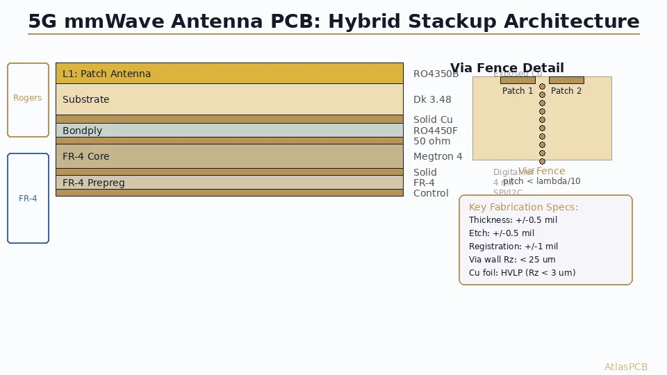
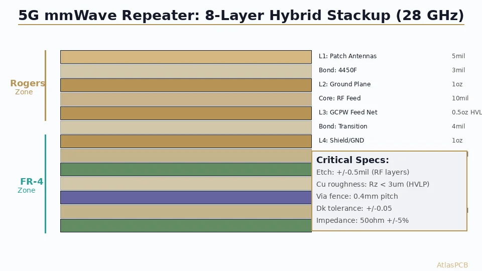
The standard approach we recommend for most 28 GHz indoor repeater designs is an 8-layer hybrid stackup:
| Layer | Material | Thickness | Cu Weight | Function |
|---|---|---|---|---|
| L1 | Rogers RO4350B | 5mil (0.127mm) | 0.5oz HVLP | Patch antenna elements |
| Bond | Rogers 4450F | 3mil | — | Prepreg (Rogers-to-Rogers transition) |
| L2 | Rogers RO4350B | — | 1oz | Ground plane (antenna cavity backing) |
| Core | Rogers RO4350B | 10mil (0.254mm) | — | Core (RF feed network operates here) |
| L3 | Rogers RO4350B | — | 0.5oz HVLP | GCPW feed network + beamformer connections |
| Bond | Rogers 4450F | 4mil | — | Prepreg (Rogers-to-FR4 transition) |
| L4 | FR-4 | — | 1oz | Ground/shield plane |
| Core | FR-4 | 12mil | — | Digital core |
| L5 | FR-4 | — | 1oz | Digital routing (beamformer control, SPI, I2C) |
| Bond | FR-4 prepreg | 4mil | — | Standard FR-4 bonding |
| L6 | FR-4 | — | 1oz | Power plane (multiple voltage domains) |
| Core | FR-4 | 12mil | — | Digital core |
| L7 | FR-4 | — | 1oz | Digital routing / power |
| Bond | FR-4 prepreg | 4mil | — | Standard FR-4 bonding |
| L8 | FR-4 | — | 1oz | Ground / components |
The key design decision is where to place the material transition boundary between Rogers and FR-4. The rule: every copper layer that carries signals at or near 28 GHz (antenna elements, feed network, beamformer chip RF connections) must be on Rogers. Everything else — digital control, power distribution, non-RF component connections — goes on FR-4 to minimize cost.
The L3 layer deserves special attention. This is where the GCPW (Grounded Coplanar Waveguide) feed network runs from the beamforming IC outputs to the L1 antenna elements via RF transitions. GCPW on 10mil Rogers with ground planes above (L2) and below (L4) provides excellent isolation and impedance control. The 50-ohm GCPW geometry at 28 GHz on RO4350B (Dk 3.48) requires approximately 8-9mil signal trace width with 4-5mil gaps to coplanar ground — all within standard manufacturing tolerances at our facility.
Critical Fabrication Tolerances at 28 GHz
At millimeter-wave frequencies, manufacturing tolerances that are negligible at lower frequencies become performance-limiting. Understanding which tolerances matter most helps you specify correctly without over-constraining (and over-paying).
Etch tolerance (most critical): +/-0.5mil required. A 50-ohm GCPW trace at 28 GHz on 5mil RO4350B is approximately 8.5mil wide. A +/-1mil etch variation (common at relaxed facilities) produces impedance swing from 44 to 56 ohms — a 12% deviation that directly impacts return loss and EVM. At +/-0.5mil, impedance stays within 47-53 ohms (+/-6%), which maintains S11 below -15 dB across the operating band.
Our standard etch process for mmWave boards uses DES (Develop-Etch-Strip) with inline optical inspection measuring trace width at 4 points per panel. Panels exceeding +/-0.5mil tolerance on RF layers are rejected before lamination — catching the issue early before expensive Rogers material is wasted in subsequent processing steps.
Copper roughness (second most critical): Rz below 3um mandatory. At 28 GHz, the skin depth in copper is approximately 0.4um. Surface roughness creates effective path elongation that increases conductor loss proportionally. Standard ED copper (Rz 5-8um) adds 0.8-1.2 dB/cm of excess conductor loss at 28 GHz compared to smooth copper. HVLP copper (Rz 1.5-2.5um) reduces this to 0.2-0.4 dB/cm excess loss.
For a repeater design with 30mm total RF trace path from beamformer to antenna, the copper roughness choice determines whether you add 2.4-3.6 dB of excess loss (ED copper) or 0.6-1.2 dB (HVLP copper). At 28 GHz, that 2+ dB difference in a repeater directly impacts link budget — potentially requiring a higher-power (more expensive, hotter) PA to compensate.
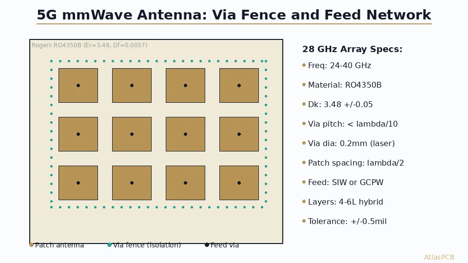
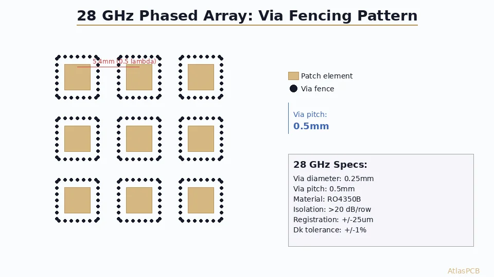
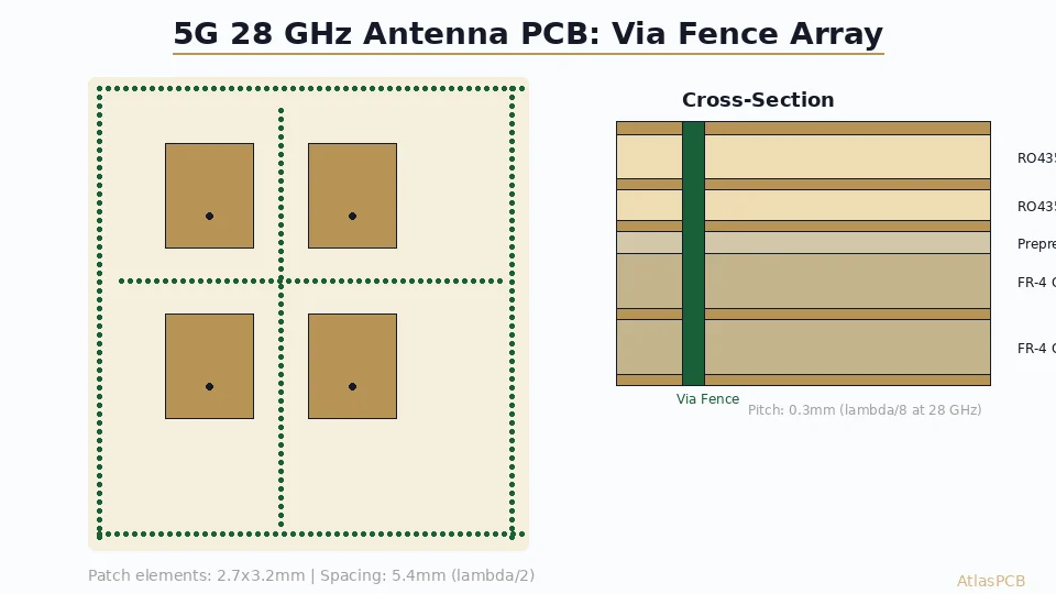
Layer-to-layer registration: +/-2mil for via fence alignment. Via fencing at 0.4mm pitch (required for lambda/10 isolation at 28 GHz) means via centers are spaced only 0.4mm apart with 0.2mm drill diameter — leaving only 0.2mm (8mil) between via edges. Layer registration error reduces effective isolation by creating gaps in the via fence wall. At +/-2mil registration, worst-case gap expansion is 4mil (from 8mil to 12mil nominal spacing), which maintains adequate isolation. Worse registration creates resonant slots that leak energy.
Drill diameter tolerance: +/-0.025mm (1mil) for via fence. Via fencing requires consistent hole diameter to maintain uniform wall spacing. Oversized holes (from drill wear) can merge adjacent vias, while undersized holes reduce plating coverage and increase via resistance. Our drill program monitors diameter with automatic tool replacement every 2000-3000 hits for 0.2mm drill bits in Rogers material (which wears tools faster than FR-4).
CHINA RF PCB MANUFACTURER
mmWave PCB Fabrication with VNA Verification
Our RF line achieves +/-0.5mil etch tolerance with HVLP copper on Rogers. Every panel includes S-parameter test coupon measurement to 40 GHz.
Request RF PCB Quote ›Antenna Element Fabrication Considerations
Indoor mmWave repeaters typically use PCB-integrated patch antenna arrays — 4x4 or 8x8 elements operating at 24-28 GHz with approximately 12-18 dBi array gain. The antenna elements are etched copper patches whose resonant frequency is directly determined by three PCB manufacturing parameters: patch dimension (etch accuracy), substrate thickness, and substrate Dk.
At 28 GHz on RO4350B (Dk 3.48), a half-wave rectangular patch is approximately 3.0mm x 2.4mm (for linear polarization). The resonant frequency sensitivity to dimension is approximately 150 MHz per 0.1mm of patch dimension change. With our +/-0.5mil (0.0127mm) etch tolerance, the frequency shift from etching variation is approximately +/-19 MHz — acceptable for the typical 400 MHz bandwidth requirement of n257/n258 bands.
However, Dk variation between production panels is the dominant source of resonant frequency shift for antenna elements. On Rogers 4350B with specified Dk tolerance of +/-0.05, the resonant frequency shift is approximately +/-200 MHz — significantly larger than the etch contribution. This means antenna bandwidth design must account for +/-200 MHz of production variation, effectively requiring antenna elements with 800+ MHz bandwidth (400 MHz operational plus 200 MHz on each side for production tolerance). Aperture-coupled patch elements or stacked patch designs achieve this bandwidth requirement more readily than single-layer patches.
Selective solder mask removal over antenna elements is mandatory at 28 GHz. Solder mask (Dk 3.5-4.2, thickness 15-25um) acts as an uncharacterized superstrate over the antenna that shifts resonant frequency down by 200-400 MHz and introduces additional loss of 0.3-0.5 dB per element. Specify mask openings extending at least 0.5mm beyond antenna element boundaries in all directions.
Production Yield and Test Strategy
mmWave repeater PCBs have inherently lower yield than standard boards due to the tight tolerance requirements. Based on our production data from Q1-Q3 2026:
| Board Type | Typical First-Pass Yield | Main Failure Mode |
|---|---|---|
| Standard 8-layer FR-4 | 92-95% | Open/short defects |
| 8-layer hybrid Rogers/FR-4 (sub-6 GHz) | 88-92% | Impedance out of spec |
| 8-layer hybrid (28 GHz repeater) | 80-86% | Etch tolerance + impedance |
| 12-layer full Rogers (mmWave) | 72-78% | Registration + impedance + material |
For 28 GHz repeater boards, we implement a specific test strategy:
- Per-panel TDR measurement on dedicated RF test coupons matching the GCPW geometry in the design. Pass criteria: 50 ohms +/-3 ohms (6%).
- Patch antenna resonance spot-check via VNA measurement on designated test elements on each panel (3 locations: center, corner, edge). Pass criteria: resonant frequency within +/-50 MHz of target.
- Isolation measurement between adjacent feed lines using embedded directional coupler coupons. Pass criteria: isolation better than -20 dB at 28 GHz.
- Visual inspection under 20x magnification for via fence continuity and etch defects on RF layers.
This testing adds approximately $2-3 per board in test time and coupon area (reducible at high volume with dedicated fixtures), but catches the specific failure modes that would otherwise propagate to assembled repeaters failing final RF calibration — where the cost of failure is 10-50x higher.
5G PCB FABRICATION
Prototype to Production for 5G mmWave Repeaters
Rogers 4350B hybrid stackups with per-panel RF verification. Engineering DFM review for mmWave designs included with every order.
Manufacturer Qualification for mmWave Repeater PCBs
Not every PCB manufacturer claiming “RF capability” can produce 28 GHz repeater boards reliably. Based on our experience qualifying suppliers in the China PCB ecosystem, here are the specific capabilities to verify:
Material sourcing: Confirm the manufacturer procures Rogers directly from authorized distributors (AGC/Rogers official channel) — not grey market. Grey market Rogers material may have incorrect date codes, improper storage conditions (humidity absorption degrades Df), or lot-to-lot Dk variation exceeding specification. Request material certificates with lot numbers for your specific order.
Process capability at your geometry: Ask for Cpk data on etch tolerance for trace widths matching your design (8-10mil for 28 GHz GCPW). A Cpk above 1.33 indicates the process consistently meets +/-0.5mil tolerance. Many shops achieve +/-1mil routinely but cannot demonstrate +/-0.5mil capability — which is the difference between working and non-working 28 GHz boards.
VNA measurement capability to 40 GHz: Request a sample measurement report showing S-parameter data on test coupons matching your stackup. If the manufacturer can only test to 8 GHz (common), they cannot verify 28 GHz performance and are essentially flying blind on your production boards.
HVLP/VLP copper availability: Confirm they stock or can source HVLP copper foil (Rz < 3um) in the weights you need (typically 0.5oz for antenna layers, 1oz for ground). Many shops only stock standard ED copper and will not flag the roughness issue unless you specifically request low-profile foil.
ATLASPCB
Ready to Fabricate Your 5G mmWave PCB?
We specialize in Rogers hybrid stackups for 5G repeater, base station, and antenna applications. HVLP copper, +/-0.5mil etch, VNA-verified to 40 GHz. Upload your design for engineering review and quotation.
Upload Design Files ›
Reviewed by AtlasPCB Engineering Team — 15+ years in advanced PCB fabrication for RF, HDI, and rigid-flex applications.
Related Reading:
About AtlasPCB — We specialize in complex PCB manufacturing for HDI, RF, and high-reliability applications. Explore our RF and high-frequency PCB services, Rogers RO4350B PCB manufacturing, or get an multilayer PCB fabrication up to 30 layers . Every order includes free engineering review. Get your quote.
Reviewed by AtlasPCB Engineering Team — IPC-certified manufacturing specialists with 15+ years of production experience in HDI, RF, and high-reliability PCB fabrication. Content based on factory floor data and real customer design reviews.
Frequently Asked Questions
What PCB material is needed for 5G indoor repeaters at 28 GHz?
How many layers does a typical 5G mmWave repeater PCB need?
What via fencing pitch is required at 28 GHz?
Can a standard PCB manufacturer fabricate 28 GHz repeater boards?
What is the typical cost for a 5G mmWave repeater PCB?
- 5G antenna PCB fabrication
- RF PCB design and manufacturing
- Rogers 4350B stackup
- China RF PCB manufacturer
- mmWave PCB