· AtlasPCB Engineering Team · Design · 13 min read
Teardrop Pad Design and Trace Necking: DFM Strategies for PCB Manufacturing Yield Improvement
Adding teardrops at pad-to-trace junctions and controlling trace neck-down geometry reduces drill breakout defects by 60 percent and improves first-pass yield for high-density PCB designs requiring 4/4 mil trace and space rules.
The Mechanical Vulnerability at Pad-to-Trace Junctions
Every pad-to-trace connection on a printed circuit board represents a potential failure point during manufacturing. Where a 4-mil trace meets a 20-mil pad, the abrupt geometric transition creates a stress concentration that is vulnerable to three distinct manufacturing hazards: drill registration error, etching undercut, and mechanical stress during depaneling. IPC-2221B Section 6.2.3 defines minimum annular ring requirements of 5 mils for external layers and 4 mils for internal layers in Class 2 designs, but even with these minimums met, the sharp intersection between trace and pad produces a geometry that is inherently more susceptible to copper cracking under thermal stress than a gradual transition.
A drill that lands 2 mils off its nominal position (well within typical CNC drilling tolerances of plus or minus 3 mils per IPC-6012) can sever a trace at its junction to a via pad if no teardrop fillet exists. At our facility, analysis of 18 months of production data shows that 43 percent of all drill breakout defects occur at pad-to-trace entry points rather than at the pad center. This statistic alone justifies the implementation of teardrop geometry as a standard DFM practice. The teardrop adds copper material at the junction point, effectively widening the trace approach into the pad and providing tolerance margin against drill wander, etch undercut, and inner layer registration shift.
Teardrop Geometry: Dimensions, Angles, and Implementation Rules
A teardrop is a tapered copper region that creates a gradual width transition between a trace and its destination pad. The standard teardrop geometry uses a 45-degree approach angle (measured from the trace centerline to the pad edge), with the teardrop length extending 1x to 2x the trace width beyond the pad edge. For a 5-mil trace entering a 25-mil pad, the teardrop would start approximately 5 to 10 mils from the pad edge and widen linearly to blend into the pad circumference. This simple geometry adds only 0.2 to 0.5 square mils of copper area per junction but provides enormous manufacturing margin improvement.
The two common teardrop shapes are linear (straight-sided) and arc-based (curved transition). Linear teardrops are simpler to implement in CAD systems and work well for trace widths above 5 mils. Arc-based teardrops provide smoother current flow and reduced impedance discontinuity for high-speed signals, making them preferred for applications above 10 GHz where even small geometric discontinuities create measurable reflections. Cadence Allegro, Altium Designer, and Siemens Xpedition all provide automated teardrop generation tools, typically applying teardrops to all pad entries with a single command. The Allegro “Add Teardrop” command processes an entire design in under 30 seconds and offers parametric control over teardrop length, width, and style. We recommend that customers apply teardrops before generating manufacturing output files, as retroactive addition at the CAM stage requires manual editing and risks introducing design rule violations.
Quantifying Yield Improvement from Teardrop Implementation
The yield impact of teardrop implementation varies with design density and drill technology, but the improvement is consistently measurable across all board types. For standard multilayer boards with 8-mil minimum trace width and 12-mil vias, teardrop addition improves first-pass electrical test yield by 2 to 4 percent. While this percentage appears modest, it translates to significant cost savings at production volumes. A 3 percent yield improvement on a panel yielding 20 boards per panel means recovering 0.6 boards per panel that would otherwise require repair or scrapping. At monthly volumes of 500 panels, this represents 300 additional good boards per month.
For high-density designs with 4/4-mil trace and space rules, the yield improvement from teardrops increases to 5 to 8 percent because tighter geometries leave less margin for drill registration error. Our production records from Q1 2026 show that designs submitted with teardrops already applied achieved 97.8 percent first-pass electrical yield, compared to 91.4 percent for geometrically identical designs without teardrops, controlling for the same layer count, material, and minimum feature size. The 6.4 percent difference directly correlates with reduced drill breakout and etch-induced opens at pad junctions. IPC-6012 Class 3 production requires 100 percent electrical testing, meaning every defect must be found and either repaired or scrapped, making yield improvement directly measurable and economically significant.
Trace Neck-Down: Managing Width Transitions at BGA Breakouts
Trace necking refers to the controlled reduction of trace width as it transitions from routing space into the constrained area between BGA pads. A 1.0mm pitch BGA with 0.5mm pads and dog-bone via breakout leaves approximately 0.2mm (8 mils) between adjacent pad edges for trace routing. If the standard trace width in the routing channel is 5 mils, the trace may need to neck down to 3.5 mils to pass between pads with adequate clearance. This width transition must be designed carefully to avoid creating impedance discontinuities, etch-related opens, and stress concentration points.
The neck-down should occur gradually over a distance of at least 3x the trace width change. Reducing from 5 to 3.5 mils (a 1.5-mil reduction) requires a transition length of at least 4.5 mils, producing a taper angle of approximately 18 degrees. Sharper angles create localized current crowding that increases resistive heating and, more critically for manufacturing, produces acute copper features that are vulnerable to over-etching. IPC-2221B does not specify maximum taper angles explicitly, but our manufacturing experience indicates that angles below 30 degrees (measured from the trace edge to the centerline) produce consistently manufacturable results across both subtractive etch and MSAP (Modified Semi-Additive Process) fabrication methods.
Impedance Impact of Teardrops and Neck-Downs on High-Speed Signals
For signals operating below 5 GHz, standard teardrops introduce negligible impedance discontinuity. The teardrop region is electrically short relative to the signal wavelength, and the brief capacitive loading from the additional copper amounts to less than 0.05 pF per junction. However, at 28 GHz (typical for 5G mmWave applications) or in 112 Gbps PAM4 SerDes channels, even small geometric transitions create measurable reflections. Time-domain reflectometry (TDR) measurements show that a standard 45-degree teardrop on a 4-mil trace creates a local impedance dip of 1.5 to 3 ohms in a 50-ohm system, lasting approximately 5 picoseconds.
For these high-speed applications, arc-based teardrops with longer transition lengths (3x to 5x trace width) reduce the impedance perturbation to below 1 ohm, keeping the reflection coefficient below 0.01 which is generally considered negligible for channel margins. Ansys HFSS and Keysight ADS simulations can quantify the exact impact for specific geometries. Similarly, trace neck-downs in BGA breakout regions create brief impedance increases (because narrower trace means higher impedance for microstrip and stripline), which can be partially compensated by reducing the reference plane spacing locally or by widening the neck-down region with copper fills. Our signal integrity team runs full-wave simulations for all designs operating above 25 Gbps per lane to verify that cumulative reflections from teardrops and neck-downs remain within the IEEE 802.3 channel compliance mask.
Etching Considerations: How Feature Geometry Affects Etch Uniformity
The etching process inherently attacks copper from all exposed surfaces simultaneously, creating the well-known trapezoidal cross-section where trace bottom width exceeds top width. This etch undercut, typically 0.3 to 0.8 mils per side for standard alkaline ammoniacal etchant at 2-ounce copper weight, has different effects on uniform trace segments versus geometric transitions. At a sharp pad-to-trace junction without a teardrop, etch undercut from the pad side and the trace side meet at an acute angle, creating a wedge-shaped copper reduction zone that can thin the effective trace width by an additional 0.5 to 1.0 mil beyond the normal undercut.
With teardrop geometry, the tapered copper provides additional material that accommodates etch undercut without reducing the effective trace width below minimum requirements. For a 4-mil trace with 0.5-mil per side undercut, the effective width after etching is 3.0 mils. If drill registration error removes 1.5 mils of the annular ring on one side, the remaining copper at the junction could be as narrow as 1.5 mils without a teardrop. With a 45-degree teardrop providing 2 mils of additional width at the junction, the worst-case minimum copper width increases to 3.5 mils, well above the IPC-6012 Class 3 minimum conductor width reduction threshold of 20 percent. Our etch compensation tables account for teardrop presence, applying 0.3-mil less compensation at teardroped junctions compared to bare junctions because the additional copper already provides manufacturing margin.
Inner Layer Registration and How Teardrops Compensate for Alignment Tolerance
Multilayer PCB manufacturing introduces layer-to-layer registration error that accumulates through the lamination and drilling processes. IPC-6012 Class 3 allows maximum 3-mil registration error between any inner layer and the drilled hole pattern. In a 16-layer board with 0.3mm vias targeting 0.15mm pads on inner layers 4 through 13, this 3-mil tolerance consumes a significant portion of the available annular ring. Without teardrops, a 3-mil registration error combined with 0.5-mil etch undercut can completely sever the trace-to-pad connection on inner layers where pad diameters are minimized to maintain routing density.
Adding teardrops to inner layer pad connections extends the effective pad capture area by 30 to 50 percent in the direction of the trace approach. For a 12-mil inner layer pad receiving a 4-mil trace, the teardrop extends the copper footprint an additional 4 to 6 mils along the trace axis, providing extra capture tolerance against both X and Y registration errors. This is particularly valuable for HDI structures where inner layer pads serve as laser via targets on subsequent buildup layers. Misregistration between the laser via and the inner layer target pad is already constrained to plus or minus 25 micrometers for 100-micrometer microvias, and any additional geometric tolerance provided by teardrops directly translates to higher via reliability. At our production facility, we measure inner layer registration using optical AOI systems from Orbotech (now part of KLA) with measurement accuracy of plus or minus 0.5 mil, flagging any panel exceeding 2.5 mil shift for enhanced inspection.
CAD Implementation: Automating Teardrops Across Major EDA Platforms
Implementing teardrops effectively requires understanding each EDA tool’s automation capabilities and limitations. In Altium Designer 24, the “Teardrop” command under Tools applies arc-based teardrops to all or selected pad-to-trace junctions, with parameters for teardrop style (arc or track), length (expressed as percentage of pad diameter, typically 30 to 50 percent), and width (expressed as fraction of pad diameter). The Altium algorithm respects existing DRC clearances and will skip junctions where teardrop addition would violate spacing rules, making it safe to apply globally without manual cleanup.
Cadence Allegro applies teardrops through the Shape menu, offering both “Pad-Connect” and “Via-Connect” teardrop modes with independent parameter sets. The Allegro approach allows asymmetric teardrops where the left and right sides use different angles, useful for differential pair routing where symmetric teardrops might violate pair-to-pair spacing. KiCad 8 added native teardrop support in version 7.0, accessible through Board Setup under Design Rules, with automatic application during DRC execution. For manufacturers receiving bare Gerber files without embedded teardrop information, some CAM systems (including Genesis 2000 and InCAM) offer post-processing teardrop addition, though this approach risks introducing spacing violations that the original DRC-clean design did not contain. We strongly recommend that designers add teardrops during the design phase rather than relying on manufacturer-side addition.
Neck-Down Rules for 0.4mm and 0.5mm Pitch BGA Breakouts
Fine-pitch BGAs with 0.4mm (16-mil) and 0.5mm (20-mil) pad pitch represent the most constrained routing scenario where trace necking is unavoidable. For a 0.5mm pitch BGA with 0.275mm (11-mil) pads and via-in-pad breakout, the available routing channel between adjacent pads measures only 0.225mm (9 mils). Subtracting minimum clearances of 3 mils per side leaves 3 mils for the trace width in the neck-down region. This extreme reduction from a 5-mil routing trace to a 3-mil necked trace requires careful management to maintain manufacturability.
The critical neck-down rules for fine-pitch applications include maintaining a maximum taper ratio of 3:1 (entry width to neck width), using transition lengths of at least 5 mils for each 1-mil width reduction, and ensuring that the necked region length is minimized to less than 50 mils total. Longer necked regions increase the probability of etch-induced opens because the narrow feature has less copper to lose before becoming discontinuous. For 0.4mm pitch BGAs (currently used in advanced mobile processors and FPGA packages from AMD and Intel), the neck-down region may require MSAP or SAP fabrication rather than standard subtractive etching because 3-mil traces at 1-ounce copper weight produce etch factors exceeding 3:1 that make reliable production with subtractive processes extremely difficult. At our HDI facility, 0.4mm pitch BGA breakouts are fabricated using modified semi-additive processing with 5-micrometer seed layers, achieving 2.5/2.5-mil trace and space with etch factors below 1.5:1.
DFM Checklist: Implementing Teardrops and Neck-Downs Before Manufacturing
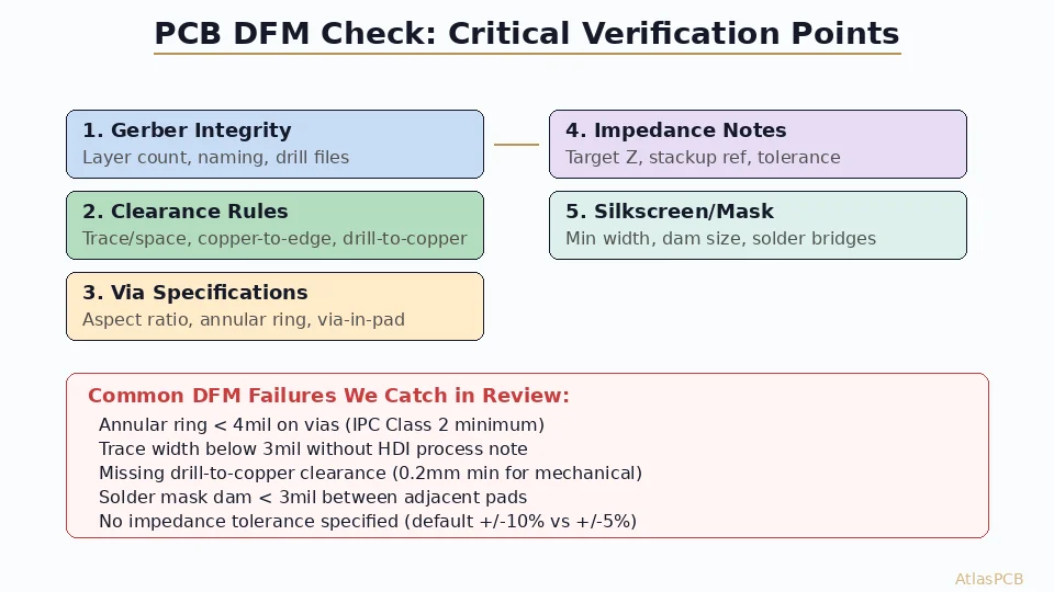
Before releasing a PCB design for manufacturing, engineers should verify the following teardrop and neck-down criteria to maximize first-pass yield. First, confirm that all pad-to-trace junctions include teardrops with minimum 30-degree approach angles (45 degrees preferred). Second, verify that all via-to-trace connections include teardrops, with special attention to blind and buried vias where registration tolerance is tighter than through-hole vias. Third, check that all trace neck-down regions maintain gradual tapers below 30 degrees with transition lengths exceeding 3x the width change.
Fourth, confirm that teardrop additions have not created DRC violations by re-running design rule checks after teardrop application. Fifth, for controlled impedance traces, verify through simulation that teardrops and neck-downs do not create reflections exceeding 5 percent of the characteristic impedance. Sixth, check that minimum copper features after neck-down remain above 3 mils for subtractive etch or 2 mils for semi-additive processing. Our DFM review team checks all six criteria for every incoming design file, providing modification recommendations within 4 hours of file receipt. Approximately 35 percent of designs we receive lack teardrops entirely, and another 20 percent have incomplete teardrop coverage (applied only to component pads but missing on vias or inner layer connections). Addressing these omissions before panel generation consistently reduces manufacturing time by eliminating the rework cycles caused by drill breakout and etch-induced open defects.
When Not to Use Teardrops: Exceptions and Trade-offs
While teardrops provide clear manufacturing benefits in most scenarios, certain situations require their omission or modification. RF circuits operating above 20 GHz with impedance-matched transmission lines may prohibit any trace width variation within matched-length segments, as the capacitive loading from teardrops can disrupt carefully tuned delay matching. In these cases, designers specify “no teardrop zones” in critical RF sections while maintaining teardrops elsewhere on the board. Similarly, current-sensing resistor connections with Kelvin (4-wire) pad geometries should not include teardrops because the additional copper area alters the resistance measurement accuracy.
Thermal relief connections to power planes represent another exception. Thermal relief spokes connecting pads to planes already incorporate geometric transitions (the spoke width and angle), and adding teardrops to spoke endpoints can create copper geometry that interferes with solder mask dam placement between the relief opening and the pad. For ground planes with full thermal connections (no relief), teardrops are unnecessary because the entire pad boundary connects directly to the copper pour. In our design review process, we identify and flag these exception cases rather than blindly applying teardrops everywhere, recognizing that manufacturing yield optimization must balance against electrical and thermal performance requirements for the specific application.
Reviewed by AtlasPCB Engineering Team
Want a Free DFM Review of Your Design?
Upload your Gerber files and our engineering team will check teardrop coverage, trace necking, and 47 other manufacturability criteria within 4 hours.
Get Your Quote →About AtlasPCB — We specialize in complex PCB manufacturing for HDI, RF, and high-reliability applications. Explore our free engineering DFM review, or get an full PCB manufacturing capabilities . Every order includes free engineering review. Get your quote.
Reviewed by AtlasPCB Engineering Team — IPC-certified manufacturing specialists with 15+ years of production experience in HDI, RF, and high-reliability PCB fabrication. Content based on factory floor data and real customer design reviews.
- teardrop design
- trace necking
- DFM
- PCB yield improvement
- annular ring
- drill breakout
- IPC-2221