· Atlas PCB Engineering Team · News · 7 min read
ZJ InnoLight Takes Strategic Stake in PCB Giant Avary Holding as AI Optical Interconnect Demand Reshapes Supply Chain
Optical transceiver leader ZJ InnoLight has acquired a 1.04% stake in Avary Holding valued at RMB 2.32 billion, becoming its fourth-largest shareholder. The investment signals deepening vertical integration between optical module and PCB manufacturers as 800G/1.6T transceiver demand drives explosive growth in substrate-like PCB and high-density interconnect technology.
Optical Meets PCB: A RMB 2.32 Billion Supply Chain Signal
The boundaries between optical interconnect and printed circuit board manufacturing are dissolving rapidly under the pressure of AI infrastructure demand. On August 11, 2026, Avary Holding disclosed in its semi-annual report that Zhongji InnoLight Investment — a wholly-owned subsidiary of optical transceiver giant ZJ InnoLight — now holds 24 million shares representing 1.04 percent of Avary Holding’s total share capital. Based on the closing price of RMB 96.67 per share on the disclosure date, this position carries a market value of approximately RMB 2.32 billion (roughly USD 320 million).
The stake makes ZJ InnoLight Investment Avary Holding’s fourth-largest shareholder, a position that transcends mere financial investment. ZJ InnoLight is one of the world’s leading manufacturers of high-speed optical transceivers for data center interconnect, currently shipping 800G modules at volume and developing 1.6T and 3.2T next-generation products. Avary Holding is among the top PCB manufacturers globally, specializing in high-density interconnect boards, substrate-like PCBs, and embedded component technology for servers, smartphones, automotive electronics, and — increasingly — optical modules themselves.
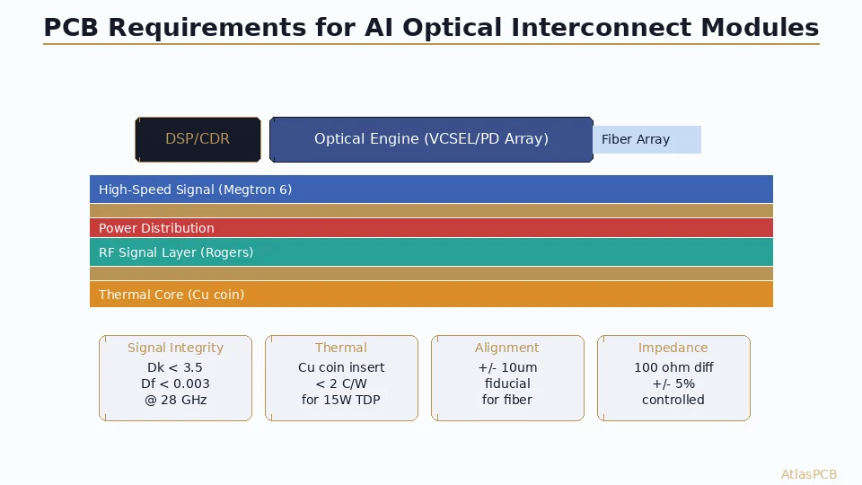
This cross-sector shareholding reflects a fundamental shift in how the AI data center supply chain is structuring itself. As optical transceiver data rates climb toward 1.6 terabits per second and beyond, the PCB substrate inside each module becomes a performance-limiting element. Signal integrity at 112 Gbps per lane PAM4 modulation demands PCB substrates with controlled impedance tolerances below plus or minus 5 percent, ultra-low-loss dielectric materials, and manufacturing precision that approaches semiconductor packaging territory.
Why PCB Technology Is the Bottleneck for Next-Generation Optics
The connection between optical transceiver performance and PCB substrate technology is not immediately obvious to engineers outside the photonics industry. Traditional optical modules used relatively simple 4 to 6 layer FR-4 PCBs as host boards, with the optical and electrical domains separated by discrete transimpedance amplifiers and laser drivers on the module itself. The PCB was merely a carrier — its electrical performance was largely irrelevant to the optical link budget.
That architecture has been obsolete for several generations now. Modern 800G optical transceivers using OSFP or QSFP-DD800 form factors integrate DSP chips running at 200 Gbps electrical lanes internally. The PCB substrate inside the module must carry these signals with insertion loss budgets measured in fractions of a decibel per centimeter. At 56 GHz Nyquist frequency for 112G PAM4, even standard low-loss FR-4 introduces unacceptable signal degradation over the 15 to 25 millimeters of trace length between the DSP and the optical engine.
This has driven optical module manufacturers toward substrate-like PCB technology — a fabrication approach that borrows techniques from semiconductor packaging to achieve trace widths below 30 micrometers, via diameters below 50 micrometers, and dielectric layer thicknesses controlled to plus or minus 5 micrometers. Avary Holding’s SLP products have already achieved qualification for 800G and 1.6T optical modules at multiple customers, with volume shipments underway.
ZJ InnoLight’s investment in Avary Holding is therefore not speculative — it is a supply chain insurance policy. As 1.6T modules enter mass production in late 2026 and 2027, the number of qualified SLP substrate suppliers becomes a critical constraint. By holding equity in a key substrate supplier, ZJ InnoLight gains both commercial leverage (preferred allocation during capacity shortages) and technical collaboration depth (early access to next-generation substrate capabilities for 3.2T development).
Avary Holding’s Financial Results Confirm the AI PCB Thesis
The numbers from Avary Holding’s first-half 2026 results tell a compelling story about where PCB industry growth is concentrating. Total revenue reached RMB 17.217 billion, up 5.14 percent year-over-year — a solid but unremarkable growth rate for the overall business. The headline figure, however, obscures what happened in the optical transceiver PCB division: sales revenue of RMB 626 million, representing approximately 11 times the revenue recorded in the same period one year earlier.
An 11-fold year-over-year increase in a single product segment is extraordinary by any measure. It reflects both the explosive ramp of AI data center construction (driving demand for 800G optical interconnect in hyperscale deployments) and Avary Holding’s successful qualification into this high-value segment after years of technology development. The optical PCB division, while still representing only 3.6 percent of total revenue, is growing at a rate that will make it a significant profit contributor within two to three quarters.
Net profit attributable to shareholders reached RMB 1.284 billion in the first half, up 4.11 percent year-over-year. The relatively modest profit growth compared to revenue growth reflects heavy investment in capacity expansion — the capital expenditure required to build SLP manufacturing lines capable of the precision these applications demand.
Massive Capacity Expansion Underway
Avary Holding is not resting on its first-mover advantage in AI-grade PCB substrates. The company has announced two major capacity expansion projects in 2026:
In March, Avary signed an investment agreement with Huai’an Economic and Technological Development Zone in Jiangsu Province to construct a high-end PCB production base valued at RMB 11 billion. The facility will primarily serve AI computing and optical transceiver applications, with planned capabilities including HDI boards with 20 or more layers, SLP with sub-30-micrometer features, and embedded die technology for next-generation compute modules.
In May, the company acquired industrial land in Shenzhen with plans to invest RMB 10 billion in an intelligent manufacturing base focused on AI high-tier SLP and flexible printed circuits. The Shenzhen location provides proximity to the Pearl River Delta’s optical module manufacturing cluster, reducing logistics complexity and enabling tighter technical collaboration with customers like ZJ InnoLight.
To fund these expansions, Avary Holding launched a refinancing plan in July seeking to raise RMB 9.6 billion through share placement. The proceeds are earmarked primarily for high-density interconnect build-up board projects tailored for AI servers and high-speed optical transceivers.
The combined investment commitment exceeds RMB 30 billion (approximately USD 4.1 billion) — a figure that rivals semiconductor fab investments and underscores just how capital-intensive advanced PCB manufacturing has become. The gap between companies producing standard multilayer boards and those competing at the SLP frontier is widening into an almost unbridgeable technological chasm.
What This Means for PCB Engineers and Procurement Teams
For engineers designing products that incorporate optical interconnect — whether inside data centers, telecommunications infrastructure, or emerging AI edge computing platforms — the ZJ InnoLight and Avary Holding convergence carries practical implications.
First, the PCB substrate inside your optical modules is increasingly a differentiated technology rather than a commodity component. Module vendors that have secured partnerships with advanced PCB substrate suppliers will deliver better signal integrity performance at higher data rates. When evaluating 800G and 1.6T optical module suppliers, asking about their substrate technology partner reveals supply chain resilience that the module specification alone does not capture.
Second, the same SLP and advanced HDI technologies being developed for optical transceivers will eventually cascade into broader applications. Server motherboards for AI accelerator cards, high-bandwidth memory interposers, and advanced packaging substrates all require similar fabrication precision. The capacity being built today for optical substrates will eventually serve these adjacent markets, potentially improving availability and reducing cost for advanced PCB applications beyond optics.
Third, the vertical integration trend suggests that PCB substrate supply for cutting-edge applications may become increasingly allocated rather than freely available on the open market. Companies that secure supply relationships early — through equity stakes, long-term agreements, or joint development partnerships — will have priority access during capacity-constrained periods.
For standard multilayer PCB applications that most hardware engineers encounter daily — 4 to 16 layer boards in FR-4 and Rogers materials — the immediate impact is limited. However, the broader industry dynamics are worth watching: as the leading PCB manufacturers direct increasing capital toward AI-grade substrates, their standard product lines may see less investment attention, potentially creating opportunities for specialized mid-tier manufacturers to capture share in the conventional PCB market.
Reviewed by AtlasPCB Engineering Team
About AtlasPCB — We specialize in complex PCB manufacturing for HDI, RF, and high-reliability applications. Explore our HDI PCB manufacturing capabilities . Every order includes free engineering review. Get your quote.
Reviewed by AtlasPCB Engineering Team — IPC-certified manufacturing specialists with 15+ years of production experience in HDI, RF, and high-reliability PCB fabrication. Content based on factory floor data and real customer design reviews.
- AI PCB
- optical transceiver
- Avary Holding
- ZJ InnoLight
- HDI
- substrate-like PCB
- supply chain