· AtlasPCB Engineering · News · 9 min read
As AI Models Scale 100x Every Two Years, Yole Maps the Shift From Compute to Communication -- and Its Impact on PCB Design
Yole Group's new white paper forecasts $112 billion in optical transceiver revenue by 2031 as AI infrastructure bottlenecks migrate from processors to interconnects, creating new demands for PCB substrates.
Reviewed by AtlasPCB Engineering Team
A new white paper from semiconductor and photonics research firm Yole Group, published September 7, 2026, argues that optical transceivers have evolved from supporting data-center infrastructure into a system-level requirement for scaling artificial intelligence. The report, titled “Photonics at the Speed of AI,” presents a framework for understanding how AI model growth is outpacing compute improvements and shifting the performance bottleneck to the communication fabric that connects thousands of processors within a single training cluster.
The implications for PCB manufacturers and designers are direct: as optical interconnect technology moves closer to the processor package, the substrate and board-level routing environment that supports these links must meet increasingly demanding signal integrity, thermal, and material specifications.
The Scaling Math Behind the Bottleneck
The core argument in Yole’s analysis rests on a stark numerical comparison. AI models are growing in computational requirements at a rate of approximately 100x every two years. Processor performance, by contrast, improves at roughly 3.3x over the same period. The gap between model demand and per-chip capability means that training clusters must deploy ever-larger numbers of interconnected processors, and the bandwidth required between those processors grows faster than any single link technology can deliver.
The result, according to Yole, is that the industry needs approximately 70x more interconnects every two years to keep pace with model scaling. This is a rate of deployment that the current optical module manufacturing base is not equipped to sustain at current yields and costs.
“AI makes photonics a system requirement, not an optional enhancement,” said Martin Vallo, senior technology and market analyst for Photonics at Yole Group. “The bottleneck is shifting from compute to communication.”
The market projections reflect this urgency. Yole forecasts the optical transceiver market to grow from approximately $10 billion in 2021 to $112 billion by 2031, representing a compound annual growth rate of about 35 percent. Hyperscaler capital expenditure is projected to reach $670 billion in 2026 alone, with a combined $5.3 trillion between 2026 and 2031.
A Four-Domain Framework for Interconnect Architecture
The white paper introduces a four-domain framework that maps the different physical scales at which optical communication operates within AI infrastructure: Scale-In, Scale-Up, Scale-Out, and Scale-Across. Each domain has distinct technology requirements, different incumbent solutions to displace, and different timelines for commercial deployment.
This framework is particularly relevant for PCB and substrate engineers because each interconnect domain imposes different requirements on the underlying board. Scale-In refers to communication within a single package or module, where co-packaged optics (CPO) technology is beginning to integrate optical engines directly into or adjacent to the processor package. Scale-Up encompasses the links within a single rack or cluster node. Scale-Out covers connections between racks within a data center. Scale-Across describes the wide-area links between data centers.
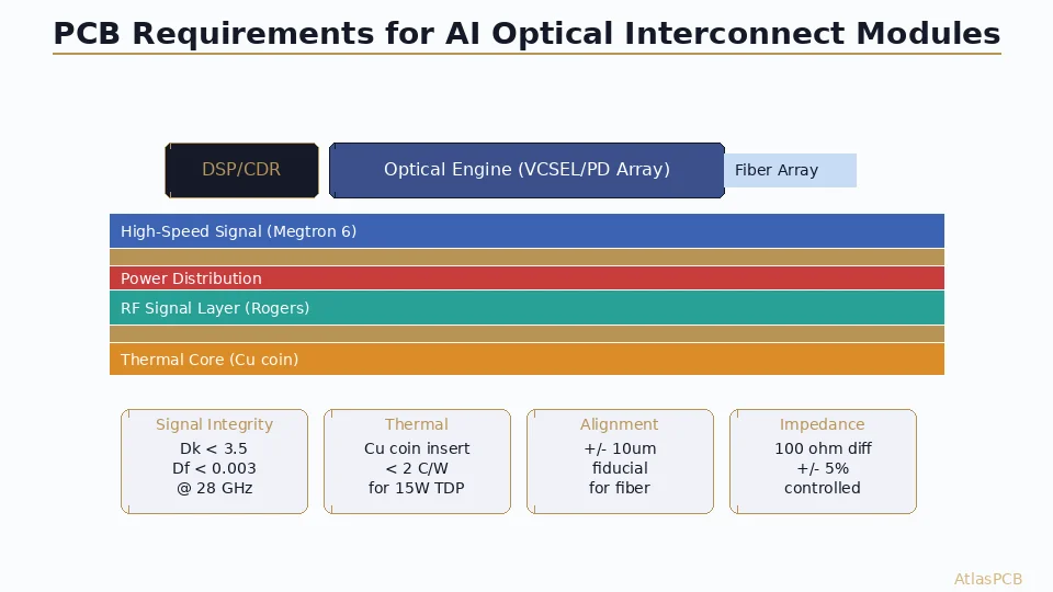
The PCB design implications vary considerably across these domains. Scale-In and Scale-Up links operate at the highest data rates and shortest distances, demanding the most stringent signal integrity on the electrical portions of the link. The host board must route extremely high-speed electrical signals from the processor to the optical engine with minimal loss and tightly controlled impedance, often through ultra-low-loss laminate materials like Megtron 6 or Megtron 7.
Building High-Speed AI Infrastructure?
AtlasPCB specializes in ultra-low-loss laminates and controlled impedance for 112G and 224G optical module host boards. Get engineering consultation and a quote in 24 hours.
Request a Free QuoteCo-Packaged Optics: From Concept to Narrow Commercial Deployment
One of the most significant technical developments tracked in the white paper is the commercial status of co-packaged optics. Yole reports that CPO is now entering commercial deployment, but narrowly — in proprietary switching platforms operated by the small number of hyperscale companies that are vertically integrated enough to absorb the manufacturing risk and yield challenges inherent in combining optical and electronic components at the package level.
The report is careful to note that this is neither a simple “copper is dying” narrative nor a “CPO will solve everything” pronouncement. Copper-based electrical links are being extended deliberately through megawatt-class rack engineering, and the transition to optical solutions is happening at different rates across different domains.
Yole’s companion market report, “Co-Packaged Optics for Data Centers 2026,” quantifies the CPO opportunity. Optical-engine revenue is forecast to grow from $0.6 billion in 2026 to $112.1 billion in 2031, with Scale-Up applications expected to capture approximately 94 percent of that market.
For PCB manufacturers, the CPO transition creates a new class of substrate requirements. The optical engine must be mounted on a substrate that provides both high-speed electrical routing for the data signals and precise mechanical alignment for fiber coupling. These substrates require tight thickness tolerances, low-loss dielectric materials, and controlled thermal expansion properties to maintain alignment across operating temperature ranges. The manufacturing processes involved — fine-line etching, precise lamination, and embedded passive components — overlap significantly with the capabilities required for advanced HDI and high-speed digital PCBs.
What This Means for PCB Material Demand
The cascade from AI model growth to interconnect demand to PCB material requirements follows a clear path. As data rates per lane increase from 100G to 200G and eventually 400G, the electrical portion of each link (even with optical conversion) demands lower insertion loss from the PCB substrate. This drives adoption of ultra-low-loss laminates — materials with dissipation factors (Df) below 0.002 at 10 GHz — for the host boards and switch boards that connect to optical modules.
The same trend is already visible in today’s AI server designs. Boards for current-generation GPU clusters commonly use 20 to 30 or more layers of low-loss or ultra-low-loss laminate, with controlled impedance tolerance of +/-7% or tighter on high-speed differential pairs. As Yole’s projections suggest, the volume of these boards will scale dramatically over the next five years, and the supply chain for advanced laminates — already under pressure from AI-driven demand — will face further strain.
Yole Group founder and president Jean-Christophe Eloy framed the challenge broadly: “The question is no longer simply which accelerators can be deployed, but whether the networking and photonic technologies required to connect them will be available at the right scale, at the right time, and at the right cost.”
That question extends directly to PCB fabrication capacity. A $112 billion optical transceiver market in 2031 implies tens of billions of dollars in associated PCB and substrate content — host boards, optical engine substrates, switch boards, and backplanes — all requiring advanced materials and tight process control.
Advanced Laminate Expertise
From Megtron 6 to Rogers high-frequency laminates, AtlasPCB processes the materials that AI infrastructure demands. Talk to our engineering team about your next project.
Request a Free QuoteThe Pluggable Optics Roadmap
Beyond CPO, the white paper maps the evolutionary path of pluggable optical modules — the more conventional form factor that remains the dominant optical interconnect technology in data centers today. Yole describes a progression through linear-drive pluggable optics (LPO), externally connected pluggable optics (XPO), and the emerging Open CPX ecosystem toward a future where optical conversion happens progressively closer to the GPU and CPU package.
Each step along this roadmap changes the PCB design requirements. LPO simplifies the electrical interface between the host ASIC and the optical module by removing the DSP retimer from the module, placing tighter signal integrity requirements on the host board traces. XPO moves the optical module outside the switch or server enclosure, potentially simplifying the thermal design of the host board but requiring longer high-speed electrical runs to the front-panel connector.
For design engineers working on next-generation AI server and switch boards, these transitions mean that PCB material selection, stackup design, and impedance control must be evaluated not just for today’s pluggable form factors but for the optical architectures that will follow. The boards being designed now for 2027-2028 production will likely need to support at least one of these transitional architectures.
Industry Context
Yole’s report arrives during a period of intense activity in AI infrastructure investment. Hyperscaler capital expenditure has been the dominant driver of growth across the semiconductor and electronics supply chain in 2026, and the PCB industry has felt the impact directly. North American PCB bookings surged 62 percent year-over-year in July 2026, according to the Global Electronics Association, with a book-to-bill ratio of 1.46 — indicating strong forward demand that is running well ahead of current shipment capacity.
The compound semiconductor supply chain is responding to the same forces. IQE, a major epitaxial wafer supplier, reported first-half 2026 revenue up 43 percent year-over-year to $64.6 million, driven primarily by AI data-center infrastructure and photonics demand. These upstream indicators suggest that the demand pipeline Yole describes is already being reflected in real purchasing activity across the electronics supply chain.
Ready for Your Project?
AtlasPCB delivers precision-manufactured PCBs for high-speed digital, RF, and AI infrastructure applications. Get a quote in 24 hours.
Request a Free QuoteSources: Yole Group White Paper “Photonics at the Speed of AI” (September 7, 2026); Yole Group market report “Co-Packaged Optics for Data Centers 2026”; Global Electronics Association North American PCB Statistical Program, July 2026; IQE plc first-half 2026 results (September 9, 2026); Semiconductor Today.
About AtlasPCB — We specialize in complex PCB manufacturing for HDI, RF, and high-reliability applications. Explore our impedance-controlled PCB manufacturing, or get an Megtron 6 & 7 low-loss PCB manufacturing . Every order includes free engineering review. Get your quote.
Reviewed by AtlasPCB Engineering Team — IPC-certified manufacturing specialists with 15+ years of production experience in HDI, RF, and high-reliability PCB fabrication. Content based on factory floor data and real customer design reviews.
- AI hardware
- optical transceivers
- data center
- co-packaged optics
- high-speed PCB
- signal integrity
- photonics