· AtlasPCB Engineering Team · News · 7 min read
SKC Injects $290 Million into Glass Substrate Subsidiary Absolics, Accelerating Next-Gen Semiconductor Packaging
South Korean materials giant SKC announces KRW 401.1 billion ($290M) rights offering for Absolics, the world's first dedicated glass substrate production facility in Georgia. Analysis of what glass substrate commercialization means for the PCB and advanced packaging supply chain.
SKC Commits $290 Million to Absolics Glass Substrate Expansion
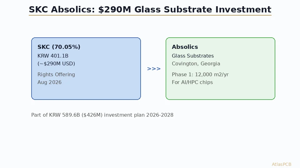
South Korean materials conglomerate SKC (011790.KS) announced on August 21, 2026 that its subsidiary Absolics Inc. will raise KRW 401.1 billion (approximately $290 million) through a rights offering to fund the next phase of glass substrate commercialization. The investment targets customer evaluations, product certification completion, yield improvement, and equipment upgrades at the company’s Covington, Georgia manufacturing facility — the world’s first dedicated glass substrate production plant.
SKC currently holds a 70.05 percent stake in Absolics, with Applied Materials holding the remaining 29.95 percent. The rights offering is part of a larger KRW 589.6 billion ($426 million) investment plan spanning 2026 through 2028, signaling that both SKC and its semiconductor equipment partner view glass substrates as a commercially viable technology ready for customer adoption rather than a research-stage concept.
The timing of this capital injection aligns with Absolics reaching critical production milestones. The company has been conducting proof-of-concept testing with undisclosed customers throughout the first half of 2026, with expanded customer evaluations planned for the second half of the year. Both embedding and non-embedding glass substrate products are undergoing reliability qualification testing, suggesting that initial commercial shipments could begin in 2027 if qualification programs proceed on schedule.
Absolics: From Concept to Production Reality
Absolics represents a decade-long bet by SKC on the proposition that glass substrates can eventually complement — and in some applications replace — the organic substrates that currently dominate semiconductor packaging. The company’s Covington, Georgia facility broke ground in 2022 with a $240 million Phase 1 investment covering 120,000 square feet of cleanroom space and an initial production capacity of 12,000 square meters per year of glass substrate panels.
The facility received $75 million in direct funding from the U.S. Department of Commerce under the CHIPS and Science Act, reflecting the U.S. government’s assessment that glass substrate manufacturing represents a strategically important capability for the domestic semiconductor supply chain. The full Phase 1 and Phase 2 master plan envisions $600 million in total investment, with Phase 2 expected to bring capacity to 72,000 square meters per year — a six-fold increase that would make Absolics a significant volume producer in the substrate market.
Applied Materials’ 29.95 percent ownership stake is particularly noteworthy because it signals semiconductor equipment industry confidence in glass substrate manufacturing feasibility. Applied Materials brings precision glass processing expertise from its display technology division, and the company’s involvement suggests that the manufacturing equipment challenges — which have been a primary barrier to glass substrate commercialization for over twenty years — are being resolved with production-worthy solutions.
Why Glass Substrates Matter for Advanced Semiconductor Packaging
Glass substrates address fundamental physical limitations of organic substrates (typically ABF-based build-up films from Ajinomoto) that become increasingly problematic as chip packages grow larger and interconnect density increases. The primary advantages of glass over organic substrates center on three material properties: dimensional stability, thermal expansion matching, and surface planarity.
Organic substrates suffer from warpage and dimensional instability that worsens with package size. As AI accelerator packages push past 2,500 square millimeters — approaching the size of a full reticle — maintaining planarity across the substrate becomes extraordinarily difficult with organic materials. Glass offers superior dimensional stability due to its rigid, amorphous structure, enabling larger package sizes with tighter interconnect pitch without the warpage management challenges that currently limit organic substrate scaling.
The coefficient of thermal expansion (CTE) of glass can be engineered to closely match silicon (approximately 3 ppm per degree Celsius), whereas organic substrates typically have CTE values of 12-17 ppm per degree Celsius that create thermal stress at solder joints during temperature cycling. This CTE mismatch between silicon die and organic substrate is a primary reliability failure mechanism in large packages — glass substrates could dramatically improve thermal cycling reliability by reducing the mechanical stress that drives solder fatigue.
Glass also enables finer line and space geometries than current organic substrates. While leading-edge organic substrates achieve approximately 2 micrometer line/space with semi-additive processing, glass substrate processes target sub-2 micrometer features enabled by the exceptional surface smoothness of polished glass (sub-nanometer roughness compared to the 200-500 nanometer roughness typical of organic substrates).
The Competitive Landscape: Where Glass Fits
Absolics is not operating in isolation. Multiple companies are pursuing glass substrate technology, though none have reached the dedicated production facility stage that Absolics achieved. Shinko Electric, an Fujitsu subsidiary, announced 22-layer glass substrate development earlier this year. Intel has been researching glass substrates for high-density interconnect applications and disclosed functional prototype results. Samsung’s packaging division has explored glass-based interposer concepts for HBM integration.
However, the current market for advanced packaging substrates remains overwhelmingly organic. Ibiden, Shinko, Samsung Electro-Mechanics, and several Taiwanese and Japanese companies supply the ABF substrates used in virtually all current AI accelerator packages (NVIDIA H100/B200, AMD MI300, Google TPU). Glass substrates are not expected to replace these organic solutions immediately but rather to enable a new tier of packaging performance that organic materials cannot achieve — particularly for the next generation of AI accelerators expected to arrive in 2027-2028 that demand even larger package sizes and higher interconnect density.
What This Means for PCB Engineers and the Substrate Supply Chain
For engineers working with current PCB and substrate technology, glass substrate commercialization carries several implications that are worth tracking even though glass will not directly replace conventional PCBs for most applications.
The technology primarily targets the advanced packaging layer — the substrate that sits between the silicon die and the printed circuit board in modern BGA and flip-chip packages. Glass substrates would compete with or complement organic substrates in this interposer/substrate layer, not with the main PCB itself. However, the interface between package substrate and PCB will need to evolve as package sizes and pin counts increase with glass substrate enablement.
Current PCB designers working on boards for high-performance AI systems already contend with the challenges of mounting extremely large BGA packages — warpage management during reflow, fine-pitch pad arrays with 0.4mm pitch or tighter, and high-density via breakout patterns beneath package footprints. If glass substrates enable even larger packages with even more I/O pins, the PCB routing and via density requirements beneath those packages will intensify further.
From a supply chain perspective, the emergence of a dedicated glass substrate production facility in Georgia diversifies the geographic concentration of advanced substrate manufacturing, which currently depends heavily on facilities in Japan, South Korea, and Taiwan. For hardware companies managing supply chain risk, a U.S.-based substrate source (supported by CHIPS Act funding) adds a domestic option for advanced packaging components — relevant for defense and automotive programs with domestic content requirements.
The PCB industry should also monitor whether glass substrate processes eventually migrate toward larger panel sizes that could benefit other aspects of electronics manufacturing. Current organic substrate production uses relatively small panels compared to PCB fabrication, which limits throughput and increases cost. Glass processing technology from the display industry routinely handles Generation 8 panels (2200mm x 2500mm), and if this panel-size advantage transfers to substrate manufacturing, it could fundamentally change the economics of advanced substrate production.
Investment Timeline and Market Readiness
The 2026-2028 investment timeframe described in SKC’s announcement suggests that commercial revenue from glass substrates is not expected before 2027 at the earliest, with meaningful volume likely in 2028-2029. The current $290 million raise specifically targets “customer evaluations, certification, and yield improvement” — language that confirms Absolics is in the qualification phase rather than volume production.
For PCB industry participants, this timeline means that glass substrates remain a medium-term technology shift rather than an immediate disruption. The organic substrate supply chain will continue serving the AI accelerator market for the current and next generation of products. However, hardware architects designing platforms with 2028-2029 production targets should begin evaluating whether glass substrate availability could enable package architectures that are currently constrained by organic substrate limitations.
The convergence of SKC’s capital commitment, Applied Materials’ ongoing partnership, CHIPS Act government funding, and active customer qualification programs suggests that glass substrates have moved beyond the research curiosity stage into a serious commercial trajectory. Whether the technology achieves broad adoption or remains confined to the most demanding high-performance applications will depend on yield economics, reliability qualification results, and the willingness of major customers (likely NVIDIA, AMD, or hyperscale cloud providers) to qualify glass substrates into their production supply chains.
Reviewed by AtlasPCB Engineering Team. Sources: Seoul Economic Daily (Aug 21, 2026), Korea Herald, The Elec, ic-pcb.com. Investment figures converted at approximately KRW 1,383 per USD.
About AtlasPCB — We specialize in complex PCB manufacturing for HDI, RF, and high-reliability applications. Explore our impedance-controlled PCB manufacturing . Every order includes free engineering review. Get your quote.
Reviewed by AtlasPCB Engineering Team — IPC-certified manufacturing specialists with 15+ years of production experience in HDI, RF, and high-reliability PCB fabrication. Content based on factory floor data and real customer design reviews.
- glass substrate
- semiconductor packaging
- SKC Absolics
- advanced packaging
- AI chips
- CHIPS Act
- substrate technology