· AtlasPCB Engineering Team · News · 7 min read
SEMICON Taiwan 2026 Opens With Record 1,300 Exhibitors as Advanced Packaging Reshapes PCB Substrate Demand
SEMICON Taiwan 2026 opens September 2-4 in Taipei with record attendance. Advanced packaging technologies including fan-out panel-level packaging and chiplet architectures are driving new demands for PCB substrate materials, with implications for PCB designers and buyers across the supply chain.
Reviewed by AtlasPCB Engineering Team
Record-Setting Exhibition Reflects Semiconductor Industry Momentum
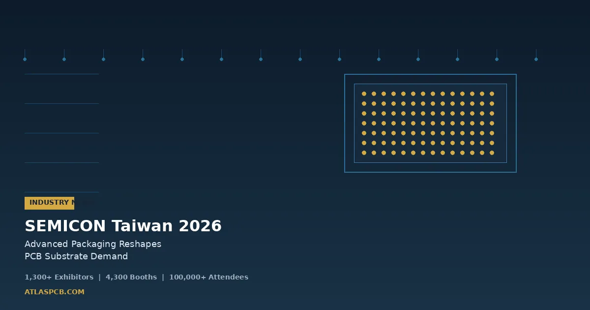
SEMICON Taiwan 2026, one of the global semiconductor industry’s most important annual gatherings, opened on September 2 at the Nangang Exhibition Center in Taipei. Running through September 4, the exhibition has set new records for scale with over 1,300 exhibitors occupying 4,300 booths — both all-time highs for the event. The number of country pavilions has reached 18, and organizer SEMI expects more than 100,000 professionals from 65 countries to attend across the three-day event.
The exhibition is part of International Semiconductor Week, which began August 31 with technical forums before the main exhibition floor opened. The event’s growing scale directly reflects the sustained investment surge in semiconductor manufacturing and packaging infrastructure driven by artificial intelligence and high-performance computing demand.
SEMI reported that global semiconductor manufacturing equipment sales reached 135.1 billion dollars in 2025, representing a 15 percent year-over-year increase, while semiconductor materials sales climbed to a record 73.2 billion dollars, up 6.8 percent. These figures provide important context for the exhibition’s focus areas, as they signal continued capital investment across the semiconductor supply chain that ultimately drives demand for advanced PCB substrates and interconnect technologies.
Advanced Packaging Takes Center Stage
The most significant theme at SEMICON Taiwan 2026 for PCB professionals is the prominence of advanced packaging technologies, particularly fan-out panel-level packaging and chiplet architectures. These technologies are reshaping the interface between semiconductor devices and the PCB substrates that carry them, creating new requirements for materials, dimensional tolerances, and manufacturing processes at the board level.
Fan-out panel-level packaging, which uses larger rectangular panels instead of circular wafers for creating chip packages, has emerged as a key technology for next-generation AI processors. TSMC has standardized its chip-on-panel-on-substrate (CoPoS) development around a 310-by-310-millimeter panel format, with research firm TrendForce reporting pilot production targeted for 2027 and mass production planned for the second half of 2028. Taiwanese companies including TSMC, ASE Technology Holding, Powertech Technology, and display manufacturers Innolux and AUO are all developing panel-level packaging capabilities.
Powertech Technology is particularly advanced in this area, preparing for fan-out panel-level packaging mass production by mid-2027, with reports that AMD and Broadcom have already reserved most of its planned capacity. The fact that major semiconductor companies are already securing capacity at packaging houses over a year before mass production begins underscores the anticipated scale of demand.
For PCB designers and buyers, these packaging advances have concrete implications. As AI chip packages grow larger and more complex, the PCB substrates beneath them must deliver finer line and space capability, lower signal loss, and more precise layer-to-layer alignment than conventional multilayer boards require. The connection between advanced packaging substrates and PCB technology is becoming increasingly direct, as substrate-like PCB constructions using build-up materials and sequential lamination are essential for routing the high-density I/O from these advanced packages.
New Exhibition Zones Reflect Industry Direction
SEMICON Taiwan 2026 has introduced several new thematic zones that highlight emerging technology areas with direct relevance to the broader electronics manufacturing ecosystem.
The Quantum Technology Zone, debuting this year, spotlights superconductor technologies, ion trap systems, and quantum annealing approaches. While quantum computing remains in its early commercial stages, the cryo-electronic packaging and specialized substrate materials required for quantum systems represent a growing niche in advanced PCB and substrate manufacturing. The zone aims to connect quantum computing companies with government research institutions and academic partners to accelerate commercialization.
The Smart Fab Zone showcases intelligent manufacturing technologies including collaborative robots, automated material handling systems, and digital twin platforms for semiconductor fabrication. These same automation and process control concepts are increasingly relevant to PCB fabrication, where lamination process control and automated inspection are becoming standard capabilities at leading manufacturers.
Perhaps most relevant for PCB professionals is the new Chiplet Pavilion within the Packaging Technology Area. Chiplet architectures — where multiple smaller dies are interconnected within a single package rather than fabricating one large monolithic die — are becoming the dominant approach for AI servers, data centers, and high-performance computing applications. The interconnect substrate that links chiplets within a package must provide extremely dense routing with low insertion loss, driving demand for high-density interconnect PCB technologies at the package substrate level that then cascade into requirements at the system board level.
PCB Substrate Materials Innovation on Display
Several major materials suppliers at SEMICON Taiwan 2026 are showcasing products that bridge the gap between semiconductor packaging and PCB manufacturing.
LG Chem is presenting its advanced packaging materials portfolio at Booth S7430, including copper-clad laminates, glass core solutions, build-up films, dry film solder resist, and photo-imageable dielectrics designed for advanced packaging processes. The company is also featuring power semiconductor materials including conductive sintering pastes and thermal interface materials based on copper metal foam for improved heat dissipation in AI data center applications. These materials represent the convergence of semiconductor packaging and PCB surface finish and material technologies, as the same material science advances are increasingly applied across both domains.
MacDermid Alpha is highlighting electrochemical materials for advanced packaging at Booth L0800, including dual damascene chemistries for complex interconnect architectures, low-alpha tin portfolios for mitigating alpha-particle-induced soft errors, and silver-alternative die attach solutions designed to reduce dependence on volatile precious metal markets. Their presentation at the TechXPOT Forum focuses on how AI and high-bandwidth memory are changing material requirements for bump coplanarity, void-free through-silicon via filling, and grain control for hybrid bonding.
ASMPT, a global technology and innovation leader in semiconductor equipment, is showcasing its advanced packaging portfolio focused on the assembly and packaging processes that connect chips to substrates. The breadth of materials and process suppliers at the event reflects how thoroughly advanced packaging has become the central technology driver for the semiconductor industry, with direct downstream effects on PCB substrate specifications and manufacturing requirements.
What This Means for PCB Buyers
The technologies on display at SEMICON Taiwan 2026 may seem distant from day-to-day PCB procurement, but they signal clear trends that will increasingly affect PCB specifications and costs over the coming years.
First, the demand for high-layer-count, tight-tolerance HDI substrates is accelerating. As chiplet-based processors become more common in commercial products beyond just AI accelerators, the PCB substrates that carry them will require capabilities that were previously limited to IC substrate fabrication houses. Fabricators who have invested in sequential lamination and microvia technology will be better positioned to serve these emerging requirements.
Second, material costs for advanced PCB applications will likely continue rising. The 73.2 billion dollar semiconductor materials market reported by SEMI includes many of the same base materials — glass fabric, specialty resins, copper foil — used in PCB fabrication. Continued capacity expansion in semiconductor packaging creates competition for these materials, supporting price levels that affect PCB fabrication costs as well.
Third, the emphasis on panel-level packaging at SEMICON Taiwan 2026 could eventually create new opportunities for PCB fabricators. Panel-level packaging uses rectangular substrates and fabrication processes that share more in common with PCB manufacturing than traditional wafer-based packaging. As this technology matures, some PCB manufacturers may find opportunities to apply their panel processing capabilities to packaging applications, blurring the historical boundary between PCB fab and semiconductor packaging.
For engineers designing products today, the practical takeaway is to stay informed about how packaging technology trends affect the PCB specifications you will need to support your next-generation designs. Working with a manufacturer that understands both the current state of multilayer PCB fabrication and the direction the industry is heading ensures your designs will be producible as packaging complexity continues to increase.
Need Advanced PCB Substrates for Next-Gen Designs?
AtlasPCB manufactures high-density multilayer PCBs with sequential lamination, microvia technology, and tight impedance control for advanced packaging applications.
About AtlasPCB — We specialize in complex PCB manufacturing for HDI, RF, and high-reliability applications. Explore our impedance-controlled PCB manufacturing . Every order includes free engineering review. Get your quote.
Reviewed by AtlasPCB Engineering Team — IPC-certified manufacturing specialists with 15+ years of production experience in HDI, RF, and high-reliability PCB fabrication. Content based on factory floor data and real customer design reviews.
Frequently Asked Questions
What is SEMICON Taiwan 2026?
How does advanced packaging at SEMICON Taiwan 2026 affect PCB designers?
What is fan-out panel-level packaging and why does it matter for PCB manufacturing?
What new technology zones are featured at SEMICON Taiwan 2026?
- semicon taiwan 2026
- advanced packaging
- pcb substrate
- fan-out panel-level packaging
- chiplet
- semiconductor industry