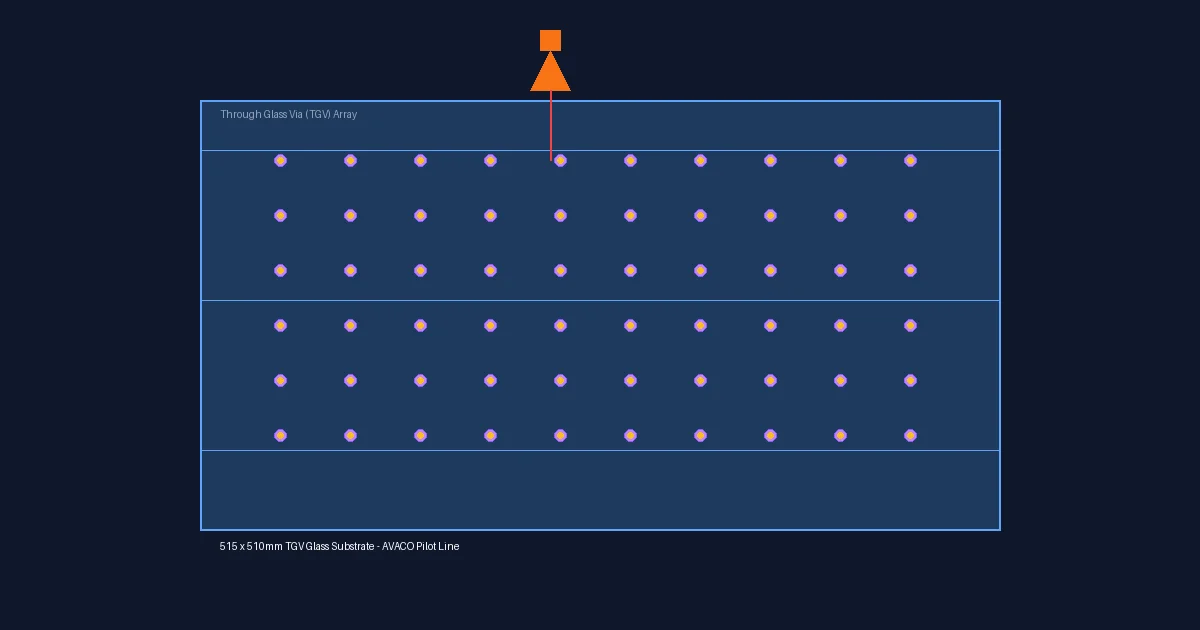
· atlaspcb-team · news · 7 min read
Huawei Targets 2027 Glass Substrate Production as China Accelerates AI Chip Packaging Race
Huawei has established a roadmap to commercialize glass substrates for AI accelerator packaging by 2027, partnering with BOE, Visionox, and other Chinese suppliers. The timeline undercuts South Korean competitors aiming for 2028+ and signals China's aggressive push to develop domestic alternatives to organic ABF substrates for next-generation AI semiconductor packaging.
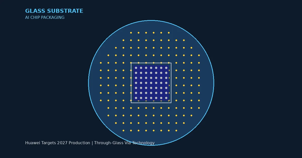
Huawei Establishes 2027 Glass Substrate Commercialization Timeline
Huawei is accelerating plans to bring semiconductor glass substrates into commercial production by 2027, according to industry sources reporting in late August 2026. The Chinese technology company has built a supply chain roadmap that would see partner manufacturers begin glass substrate production next year, primarily targeting Huawei’s AI accelerator product lines. The timeline is notably aggressive — approximately one year ahead of South Korean competitors including Samsung Electro-Mechanics, which have generally indicated mass production readiness after 2028.
The strategic significance of this development extends far beyond a single company’s procurement timeline. Glass substrates represent the next major material transition in semiconductor packaging, offering larger panel sizes, tighter wiring density, and superior dimensional stability compared with the organic ABF (Ajinomoto Build-up Film) substrates that currently dominate advanced IC packaging. For the PCB and substrate industry, this transition signals a fundamental manufacturing process shift that will reshape supply chains, equipment requirements, and competitive dynamics over the next five years.
Chinese Supplier Ecosystem Takes Shape
Huawei’s reported manufacturing partners include several major Chinese display and materials companies that are redirecting their glass processing capabilities toward semiconductor applications. BOE Technology Group, China’s largest flat panel display manufacturer, brings extensive experience in precision glass processing, thin-film deposition, and large-format panel handling — skills directly transferable to glass substrate fabrication. Visionox Technology, another display industry leader, is reportedly developing through-glass via (TGV) processing capabilities that enable the vertical electrical connections required for multi-layer substrate architectures.
Additional ecosystem participants include Yuntian Semiconductor and AKM Meadville, companies that bridge the gap between glass processing and traditional PCB/substrate manufacturing expertise. Industry sources indicate that multiple Chinese companies began developing glass substrate technologies and related supply chains several years ago, with pilot production lines now in place and process verification underway.
The competitive positioning is notable. While the broader semiconductor industry expects large-scale commercial AI platforms using glass substrates to emerge around 2030, Huawei’s accelerated timeline could enable China to introduce related products as early as 2028 — potentially ahead of the general market transition and before foreign competitors achieve volume production.
Through-Glass Via Technology Approaches Parity
The technical viability of Huawei’s timeline depends heavily on through-glass via (TGV) technology, which creates the vertical electrical interconnects that pass through the glass core material. Industry participants report that Chinese TGV capabilities have approached the level of leading global suppliers — a significant achievement given that TGV processing involves laser drilling, metallization of glass sidewalls, and precise diameter control at scales below 30 micrometers.
However, challenges remain in several areas that continue to delay commercialization worldwide. Plating processes for glass substrates differ substantially from those used for organic substrates — glass’s non-porous, chemically inert surface requires different seed layer approaches and electroplating chemistry. Micro-crack control during processing is another shared industry challenge, as the brittle nature of glass makes it susceptible to fracture propagation from process-induced defects during thermal cycling or mechanical handling.
These challenges are not unique to Chinese manufacturers — they represent fundamental physics and materials science problems that every glass substrate developer must solve. The question is whether Huawei’s ecosystem can achieve sufficient yield rates and reliability levels for commercial deployment within the aggressive 2027 timeframe.
Investment Activity Accelerates Across the Ecosystem
The pace of investment in Chinese glass substrate capabilities has intensified in recent weeks. On July 29, Hefei Chipmore Technology (688352.SH), a Chinese semiconductor packaging company, announced a RMB 50 million (USD 7.4 million) strategic investment in Chengdu Echint Technology. The investment specifically targets glass-based advanced board-level high-density integration packaging capabilities.
Echint Technology is developing what it describes as a glass substrate-level high-density packaging facility with planned total investment of RMB 5.5 billion (approximately USD 813.6 million). The company has developed a three-layer architecture combining a top polyimide redistribution layer (RDL), a glass core with high-density TGV interconnects, and a bottom ABF wiring layer. This hybrid architecture represents a pragmatic near-term approach — using glass as the core structural and interconnect layer while maintaining familiar organic materials for the outer redistribution layers.
Echint achieved mass production of its high-density fan-out multi-chip module (FOMCM) platform in 2024, making it one of the first mainland Chinese companies to commercialize advanced board-level high-density packaging. The extension to glass substrates represents a natural evolution of these existing capabilities.
Implications for the PCB and Substrate Supply Chain
The emergence of glass substrates as a viable packaging technology has broad implications for the traditional PCB and IC substrate manufacturing industry. Glass substrates compete most directly with organic ABF substrates at the high end of the market — the advanced IC substrates used in AI accelerators, high-performance computing chips, and leading-edge mobile processors.
For conventional PCB manufacturers, glass substrates represent both a threat and an opportunity. The threat is straightforward: as glass substrates capture high-value advanced packaging applications, the addressable market for organic substrates at the premium end contracts. The opportunity lies in the supporting infrastructure — glass substrate production requires new equipment, new process chemicals, and new testing capabilities that can create adjacent business opportunities for companies with relevant expertise.
For PCB buyers and electronics OEMs, the glass substrate transition will likely proceed gradually. Near-term (2027-2028), glass substrates will appear in limited applications — primarily flagship AI accelerators where the performance benefits justify the higher cost and lower initial yields. Medium-term (2029-2031), broader adoption in high-performance computing and premium mobile applications. Mass market transition for general IC packaging remains a 2032+ timeframe by most industry estimates.
The competitive dynamic between Chinese and Korean suppliers in glass substrates mirrors the broader geopolitical competition in semiconductor supply chains. Samsung Electro-Mechanics and its glass materials partner Soulbrain are pursuing their own glass substrate development programs, while Intel has invested heavily in glass substrate research at its facilities in New Mexico and India. The question of which ecosystem achieves reliable mass production first could influence competitive positioning for years to come.
What This Means for PCB Design Engineers
While glass substrates remain an IC packaging technology rather than a traditional PCB material, their emergence affects design engineers in several practical ways. First, the substrates that connect to glass-based packages will require tighter dimensional tolerances and finer features to match the increased I/O density that glass enables. Second, the superior dimensional stability of glass (essentially zero CTE mismatch with silicon) means that warpage-related design margins may be reduced in future package-on-board assemblies. Third, the availability of larger substrate panels in glass could enable new chip-on-substrate architectures that alter board-level interconnect requirements.
For current designs, no immediate action is required. But engineers working on next-generation AI hardware platforms with 2028+ production timelines should monitor glass substrate availability from their packaging suppliers, as the technology could become a available option within their product development cycle.
Advanced Substrate and HDI PCB Manufacturing
AtlasPCB manufactures high-density interconnect PCBs with fine-pitch BGA breakout, sequential lamination, and laser-drilled microvias — the board-level technologies that complement advanced IC packaging platforms.
Get HDI PCB QuoteReviewed by AtlasPCB Engineering Team
Market information sourced from IC&PCB Union reporting (August 2026), Chipmore Technology Co. strategic investment announcement (July 29, 2026), and industry analyst commentary on Chinese glass substrate development timelines. Technology descriptions reflect publicly available information on TGV processing and glass substrate architectures.
About AtlasPCB — We specialize in complex PCB manufacturing for HDI, RF, and high-reliability applications. Explore our impedance-controlled PCB manufacturing . Every order includes free engineering review. Get your quote.
Reviewed by AtlasPCB Engineering Team — IPC-certified manufacturing specialists with 15+ years of production experience in HDI, RF, and high-reliability PCB fabrication. Content based on factory floor data and real customer design reviews.
- glass substrates
- Huawei
- AI packaging
- advanced packaging
- ABF substrates
- semiconductor
- China manufacturing