 Telecommunications
16-Layer Rogers 4003C + High-Tg FR-4 Hybrid Stackup for IoT/Communication Module
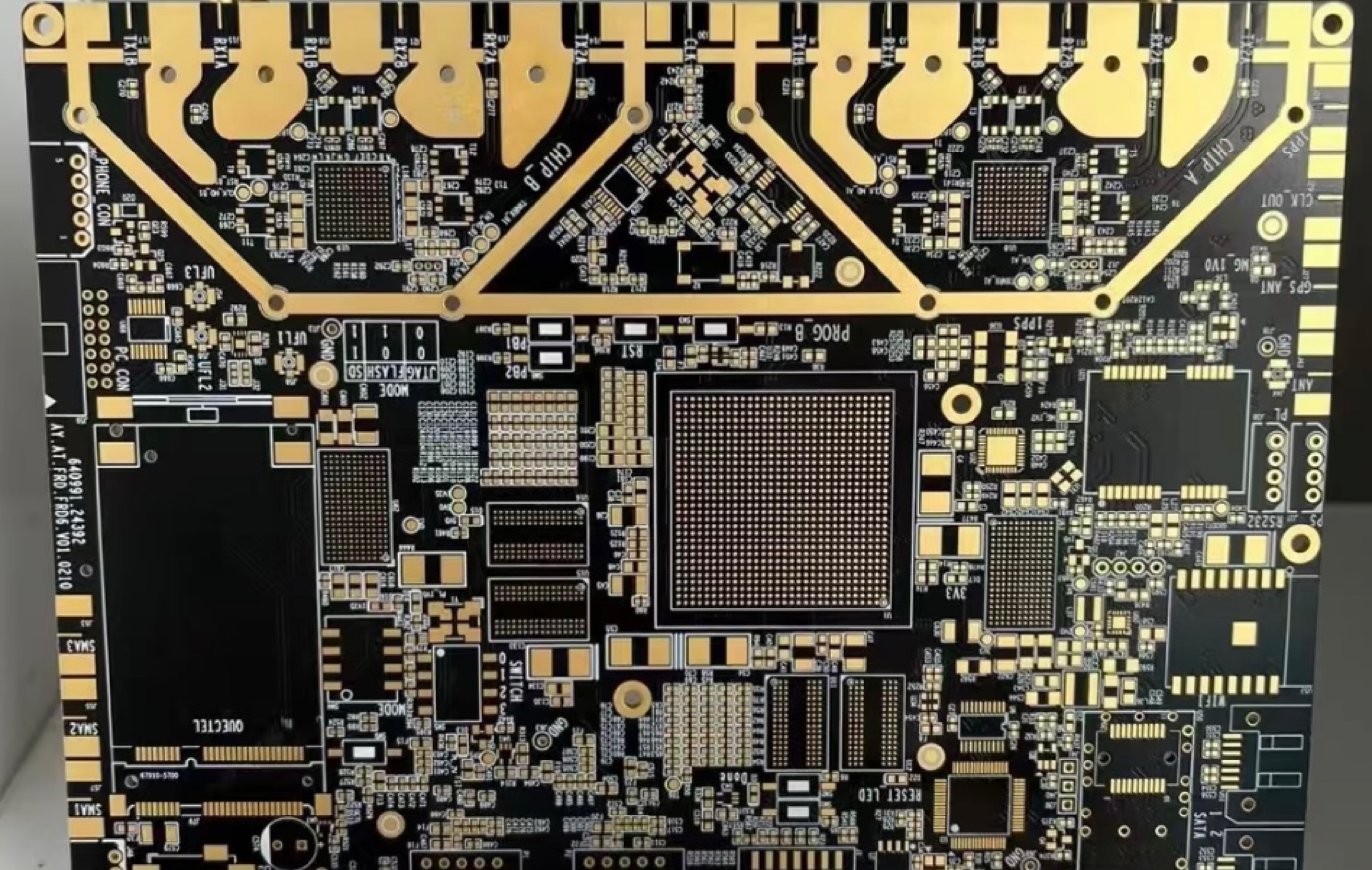
Complex 16-layer hybrid PCB combining Rogers 4003C RF laminate with TG170 FR-4 for a multi-band IoT communication module. Resin-filled vias, ENIG 2U finish, and tight thickness tolerance on a 2.17mm board.
Project Overview
A telecommunications equipment manufacturer required a high-performance 16-layer PCB for their multi-band IoT/cellular communication module. The design featured multiple RF front-ends (cellular, GPS, Wi-Fi) sharing a single board with high-speed digital processing — demanding a hybrid stackup that combined Rogers 4003C for RF layers with high-Tg FR-4 for digital signal routing and power distribution.
Challenge
The board presented several manufacturing difficulties that compound on each other in a hybrid construction:
Material compatibility in lamination. Rogers 4003C and standard FR-4 have different thermal expansion coefficients and flow characteristics. Pressing them together in a 16-layer stackup without delamination or resin starvation requires precise temperature profiling and controlled lamination pressure ramps. The CTE mismatch between Rogers (X/Y: 11/14 ppm/°C) and FR-4 (14/16 ppm/°C) creates internal stress that must be managed through symmetric stackup design.
RF performance vs. mechanical integrity. The Rogers layers needed to maintain their low-loss properties (Dk 3.38 ±0.05 at 10 GHz, Df 0.0027) while surviving the multiple press cycles inherent in a 16-layer sequential lamination. Each thermal cycle risks degrading the PTFE-glass interface if dwell times are not carefully controlled.
Resin-filled via reliability. With 16 layers and multiple RF/digital transitions, the design required extensive via stitching for ground continuity and signal transitions. All vias specified resin plugging with cap plating to enable component placement directly over via pads — critical for the dense BGA layouts of the main processor and Quectel cellular module.
Thickness control on a hybrid board. The customer specified 2.17mm total thickness with ±10% tolerance — a tight window for a hybrid stackup where Rogers and FR-4 prepregs have different compressibility and resin content. Meeting this required precise prepreg selection and validated press recipes.
Solution
Stackup design and material placement. Rogers 4003C cores placed on layers 1-2 and 15-16 (outer RF signal pairs) with high-Tg FR-4 (TG170) for the inner 12 layers handling digital routing, power planes, and ground shielding. This symmetric arrangement balances CTE stress and prevents board warpage after lamination.
Sequential lamination process. The board was fabricated using a controlled sequential press approach: inner FR-4 core first, then Rogers outer layers bonded with Rogers 4450F bondply (matched Dk/Df) in a final press cycle at reduced temperature (190°C vs typical 210°C for FR-4) to protect the Rogers material properties.
Resin plug and cap plate process. All through-hole and blind vias filled with high-Tg epoxy resin, cured, then planarized and cap-plated with 20μm copper minimum. This provided flat, solderable pads for the fine-pitch BGA components while maintaining thermal conductivity through the via barrel.
ENIG 2U surface finish. Electroless nickel (5μm) / immersion gold (0.05μm, 2 micro-inches) selected for reliable gold-wire bonding capability on the antenna pads and consistent solderability across the multiple reflow cycles required for double-sided assembly.
In-process verification. TDR impedance testing on every panel, cross-section analysis of resin-fill quality at lot boundaries, and insertion loss measurement on dedicated RF test coupons embedded in the panel array.
PCB Specifications
| Parameter | Value |
|---|---|
| Layer Count | 16 |
| Stackup Type | Rogers 4003C + TG170 FR-4 hybrid |
| RF Material | Rogers RO4003C (Dk 3.38, Df 0.0027 @ 10GHz) |
| Digital Material | High-Tg FR-4 (TG170) |
| Board Thickness | 2.17 mm |
| Thickness Tolerance | ±10% |
| Surface Finish | ENIG 2U” (immersion gold) |
| Via Process | Resin-filled, cap-plated |
| Impedance Control | Yes, ±10% (RF layers ±8%) |
| Application | Multi-band IoT/Cellular communication module |
| Special Features | Gold fingers with beveled edge, multiple SMA/UFL interfaces |
Results
- All RF channels met insertion loss specifications through 6 GHz (cellular bands, GPS L1/L5, Wi-Fi 2.4/5 GHz)
- Board thickness measured 2.15–2.19mm across production lot — well within ±10% tolerance
- Zero delamination failures after 6× reflow simulation at 260°C peak
- Resin fill quality verified >95% fill with no voids visible on X-ray inspection
- First-article passed customer functional test — all antenna ports within VSWR 2:1 specification