 Telecommunications
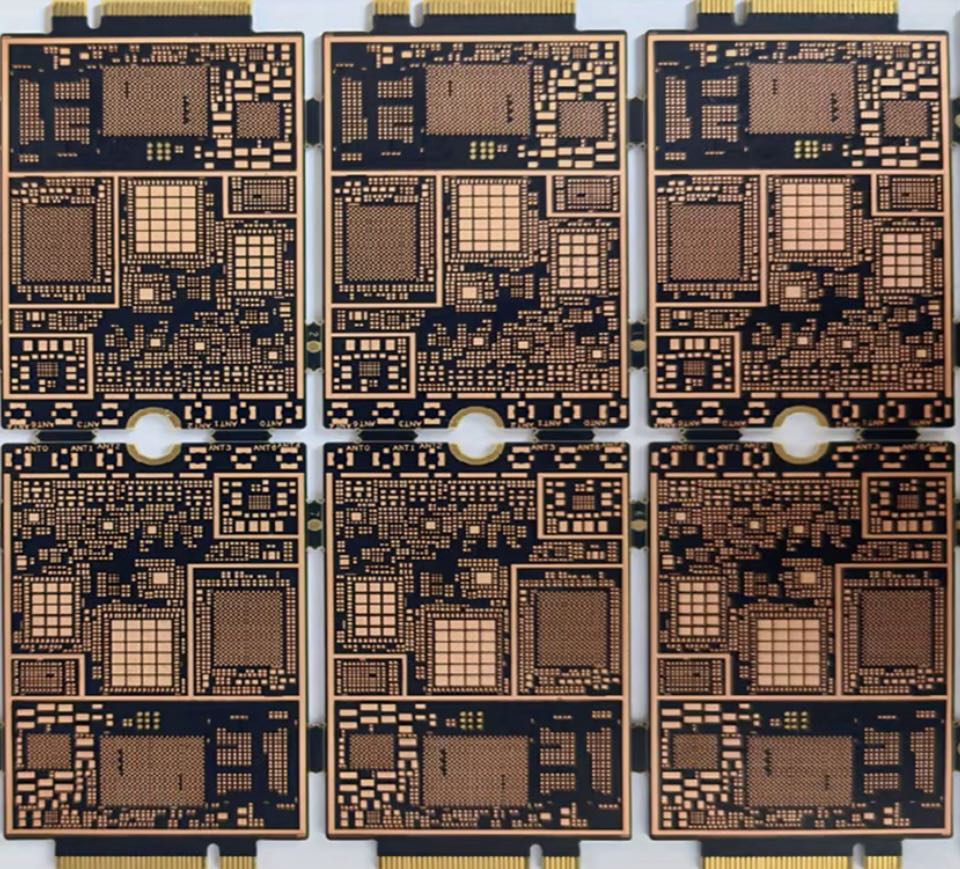
12-Layer Any-Layer HDI for Qualcomm 5G Module
Ultra-thin 12-layer any-layer interconnect HDI PCB for a Qualcomm 5G modem module. 50/50μm trace/space, 0.8mm board thickness, ENL-355 laminate with combined ENIG + OSP + gold finger surface finishes.
Project Overview
A 5G module manufacturer needed a substrate-like PCB for their Qualcomm-based 5G modem module targeting M.2 and LGA form factors. The module integrates a Qualcomm SDX series baseband processor, RF transceiver, power management, and antenna tuning — all within a compact card-edge form factor requiring gold finger connectivity. The design demanded any-layer HDI construction to achieve the routing density needed for the high-pin-count BGA packages in just 0.8mm total thickness.
Challenge
Any-layer construction at 0.8mm. Twelve copper layers with full any-layer interconnect (every layer connected to every other layer via stacked microvias) compressed into 0.8mm ±0.1mm total thickness. This gives each dielectric layer approximately 45μm average — pushing the limits of laser drilling and requiring precise resin thickness control during lamination. At this thickness, the board is extremely fragile during processing and prone to warpage without careful panel design.
50/50μm trace and space. The minimum 50μm (2 mil) features required modified semi-additive process (mSAP) or advanced subtractive etching with ultra-thin copper foil. At this geometry, copper undercut during etching becomes the dominant yield limiter. Line width uniformity must be maintained across all 12 layers despite varying etch conditions between inner and outer layers.
Three surface finishes on one board. The design specified ENIG on BGA pads for reliable solder attachment, OSP on standard SMD pads for cost efficiency, and hard gold (gold fingers) on the card-edge connector — all on the same panel. Managing selective finish application without cross-contamination requires precise masking sequences and additional process steps that increase cycle time and defect opportunities.
ENL-355 material processing. Electromagnetic New Laminate 355 (from Nan Ya / EMC) is a low-Dk, low-Df halogen-free material designed for 5G applications (Dk 3.55, Df 0.005 @ 10GHz). While it offers excellent high-frequency performance, it has different drilling and desmear characteristics compared to standard FR-4, requiring optimized laser parameters for clean microvia formation and plasma desmear recipes tuned to its resin chemistry.
Solution
Any-layer via architecture. Full stacked microvia construction with copper-filled vias at every layer transition. Each microvia drilled with UV laser at optimized parameters for ENL-355 (lower pulse energy, higher frequency vs. standard FR-4) to achieve clean hole walls without resin smear. Via diameter held to 75μm laser-drilled, filled and planarized at each sequential buildup step.
Advanced patterning process. Ultra-thin copper foil (3μm or less) with semi-additive patterning on outer layers to achieve consistent 50/50μm features. Inner layers processed with advanced subtractive etching using 12μm base copper and tightly controlled etch chemistry to maintain line width within ±8μm.
Thickness management. Precise prepreg and core thickness selection validated through trial lamination. Low-flow prepreg variants used to prevent excessive resin flow that would thin the dielectric below minimum values. Press recipe validated to achieve 0.8mm ±0.1mm consistently across the panel — verified by 9-point thickness measurement on every production panel.
Sequential surface finish application. Gold fingers processed first (electroplated hard gold, 30μ” minimum), then masked. ENIG applied selectively to BGA areas using photoimageable solder mask openings. OSP applied last to remaining exposed copper. Each transition includes cleaning and activation steps to ensure adhesion without contaminating adjacent finish zones.
Warpage control. Panel-level stress relief bake after each lamination cycle. Symmetric copper distribution enforced through dummy fills on all layers. Final boards measured <0.5% warpage per IPC-TM-650 — critical for reliable SMT assembly of fine-pitch BGAs on such a thin substrate.
PCB Specifications
| Parameter | Value |
|---|---|
| Layer Count | 12 |
| HDI Type | Any-layer (stacked microvias all layers) |
| Board Thickness | 0.8 mm |
| Thickness Tolerance | ±0.1 mm |
| Material | ENL-355 (Dk 3.55, Df 0.005 @ 10GHz) |
| Min Trace/Space | 50/50 μm (2/2 mil) |
| Microvia Diameter | 75 μm laser-drilled |
| Surface Finish | ENIG + OSP + Gold Fingers (selective) |
| Gold Finger Thickness | 30 μ” hard gold minimum |
| Application | Qualcomm 5G modem module (M.2/LGA) |
| Impedance Control | Yes, ±10% |
| Special Requirements | <0.5% warpage, halogen-free |
Results
- Achieved consistent 0.79–0.81mm thickness across production panels (within ±0.1mm spec)
- 50/50μm features held to ±8μm line width tolerance — verified on 100% AOI
- Stacked microvia reliability confirmed through 1000-cycle thermal cycling (-40°C to +125°C) with zero opens or resistance shift >10%
- All three surface finishes passed solderability testing per J-STD-002 after 4× reflow at 260°C
- Gold finger contact resistance <20mΩ after 500 insertion cycles
- RF insertion loss met Qualcomm reference design specifications through mmWave n77/n78/n79 bands