· AtlasPCB Engineering · Engineering · 20 min read
USB4 PCB Design and Fabrication: Stackup, Material, and Manufacturing Requirements for 40-80 Gbps
A PCB manufacturer's guide to USB4 board fabrication covering stackup requirements, material selection (Megtron 6, Rogers), impedance targets (85 ohm differential), trace geometry, via strategies, and real cost implications. Based on production experience with USB4 docking stations, hubs, and host controller boards.
Quick Answer
USB4 PCB fabrication requires 85 ohm ±5% differential impedance (tighter than USB 3.2's 90 ohm ±10%), low-loss dielectric materials (Dk < 3.5, Df < 0.005 at 10 GHz), minimum 6-layer stackups for Gen 3 (40 Gbps) and 8+ layers for Version 2.0 (80 Gbps), intra-pair skew under 3 mils, and back-drilled vias for any layer transition. Standard FR-4 (Df ~0.020) introduces excessive insertion loss above 10 Gbps, making mid-loss (Megtron 4, IT-180A) or ultra-low-loss (Megtron 6, Panasonic R-5575) materials mandatory. Fabrication cost runs 40-80% above standard FR-4 boards due to material premium, tighter tolerance requirements, and mandatory TDR verification with coupon testing.
Designing a PCB that reliably carries USB4 signals at 40 or 80 Gbps is fundamentally different from anything required by previous USB generations. Where USB 2.0 was forgiving enough to route on a two-layer board with standard FR-4, and USB 3.2 could work on four layers with moderate attention to impedance, USB4 demands the kind of fabrication precision traditionally reserved for high-frequency RF circuits and advanced server backplanes. The difference is not incremental. It represents a step change in what your PCB manufacturer must deliver in terms of material consistency, impedance control, and process capability.
This guide explains what USB4 requires from a fabrication perspective, based on our production experience manufacturing USB4 docking stations, Thunderbolt 4 host controllers, and multi-port USB4 hubs. We cover the specific stackup configurations, material choices, impedance targets, and manufacturing processes that determine whether your USB4 design will pass compliance testing or end up in a redesign cycle.
Understanding USB4 Signal Requirements from a Fabrication Perspective
USB4 is built on the Thunderbolt 3 physical layer, which fundamentally changes the PCB requirements compared to previous USB generations. The protocol uses two bidirectional lanes, each carrying differential signals at either 20 Gbps (Gen 3, NRZ encoding) or 40 Gbps per lane (Version 2.0, PAM-3 encoding). The combined data rate reaches 40 Gbps or 80 Gbps respectively, with an asymmetric mode pushing to 120 Gbps.
From a fabrication standpoint, the critical parameters that differ from USB 3.2 are the impedance target, tolerance band, and loss budget. USB4 specifies 85 ohm differential impedance with a tolerance of ±5% for Version 2.0 and ±7% for Gen 3. This contrasts with USB 3.2’s 90 ohm ±10% specification. The tighter tolerance alone increases fabrication complexity significantly, because achieving ±5% on differential impedance requires precise control of trace width (typically ±0.3 mil), dielectric thickness (±0.5 mil), and copper thickness (±3 microns) simultaneously across the entire panel.
The frequency content of USB4 signals extends well into the microwave range. A 20 Gbps NRZ signal has a fundamental frequency of 10 GHz, with significant energy at the third and fifth harmonics (30 GHz, 50 GHz). PAM-3 encoding at 40 Gbps per lane has a symbol rate of approximately 26.7 Gbaud, placing the fundamental around 13.3 GHz. At these frequencies, every material property, every geometric variation, and every impedance discontinuity matters.
Stackup Architecture for USB4: Layer Count and Configuration
The minimum practical layer count for USB4 depends on the design complexity and the number of USB4 ports, but the fundamental constraint is reference plane integrity. Every USB4 differential pair requires an unbroken ground reference plane on the immediately adjacent layer, with no splits, slots, or routing underneath that could disrupt the return current path.
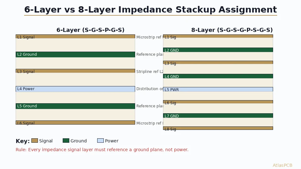
For a single-port USB4 device such as a peripheral controller, a 6-layer stackup can work if carefully designed. The recommended configuration places high-speed signal layers on layers 1 and 6 (outer layers), with ground planes on layers 2 and 5 providing continuous reference. Layers 3 and 4 handle power distribution and low-speed signals. This arrangement keeps USB4 traces as close as possible to their reference planes, minimizing the dielectric thickness and enabling practical trace widths.
For multi-port designs such as USB4 hubs and docking stations, 8 layers become the practical minimum. A typical 8-layer USB4 stackup uses the following configuration: Layer 1 carries USB4 TX pairs and high-speed signals, Layer 2 is a solid ground plane, Layer 3 handles USB 2.0 signals and low-speed control, Layer 4 provides power distribution, Layer 5 is another solid ground plane, Layer 6 carries additional USB4 RX pairs, Layer 7 is a ground plane, and Layer 8 provides a secondary signal layer for fan-out routing and ancillary circuitry.
The critical dimension in any USB4 stackup is the dielectric height between the signal layer and its adjacent reference plane. For a typical 85 ohm differential pair with 4-mil trace width and 5-mil spacing on low-loss material (Dk approximately 3.3), the required dielectric height is approximately 3.5-4.0 mils. This thin dielectric demands careful prepreg selection and precise lamination pressure control to achieve consistent thickness across the panel.
One stackup consideration that designers frequently overlook is layer-to-layer registration accuracy. At USB4 frequencies, even small misregistration between a signal trace and its reference plane can cause localized impedance variations. Our production data shows that maintaining ±2 mil layer registration is adequate for USB4 Gen 3, but Version 2.0 at 80 Gbps benefits from ±1.5 mil registration achievable with advanced inner-layer imaging and lamination alignment systems.
Material Selection: Why Standard FR-4 Cannot Support USB4
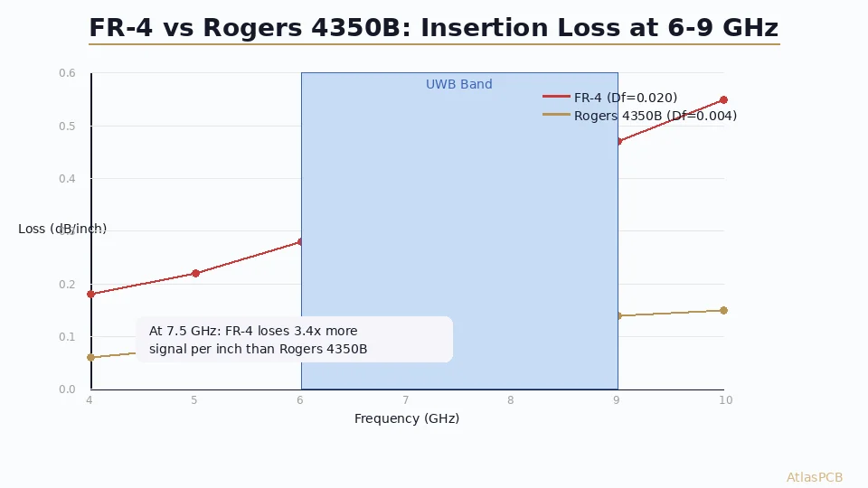
The single most important fabrication decision for a USB4 PCB is material selection. Standard FR-4 laminate, which uses dicyandiamide-cured epoxy resin with E-glass reinforcement, has a dissipation factor (Df) of approximately 0.018-0.022 at 1 GHz. This loss characteristic, which is perfectly acceptable for USB 2.0 and marginally workable for USB 3.2 Gen 1, becomes catastrophic for USB4.
Insertion loss in a PCB trace increases approximately linearly with frequency (in dB). A trace that loses 0.5 dB per inch at 1 GHz will lose roughly 5 dB per inch at 10 GHz on the same material. For a USB4 Gen 3 channel with 4 inches of total trace length (connector to chip), that translates to approximately 20 dB of insertion loss on standard FR-4 at the fundamental frequency alone. The USB4 specification allocates only about 8-12 dB of total channel loss budget for the PCB portion, making standard FR-4 physically impossible to use.
The material landscape for USB4 fabrication breaks into three tiers. The first tier covers mid-loss materials with Df between 0.005 and 0.010 at 10 GHz. This includes Panasonic Megtron 4 (R-5725, Df approximately 0.005), Isola I-Tera MT40 (Df approximately 0.005), and ITEQ IT-170GRA (Df approximately 0.007). These materials work for USB4 Gen 3 at 40 Gbps when trace lengths are kept under 4 inches and the design has minimal via transitions.
The second tier covers ultra-low-loss materials with Df below 0.004 at 10 GHz. This includes Panasonic Megtron 6 (R-5575, Df approximately 0.002), Isola Astra MT77 (Df approximately 0.002), and Nelco N7000-2 HT (Df approximately 0.003). These materials are necessary for USB4 Version 2.0 at 80 Gbps, for longer trace routing, or for designs that cannot avoid multiple via transitions.
The third tier uses Rogers or PTFE-based materials (RO4350B, RO4003C) which offer excellent high-frequency performance (Df approximately 0.004) but create significant fabrication challenges due to their different processing requirements compared to standard epoxy-glass systems. These materials are rarely necessary for USB4 and are typically reserved for 100+ GHz mmWave applications.
From a fabrication cost perspective, mid-loss materials like Megtron 4 carry a 2.5-3.5x price premium over standard FR-4, while ultra-low-loss materials like Megtron 6 command 4-6x premiums. However, the material cost impact on the finished board price is moderated by the fact that material represents only 30-40% of total PCB fabrication cost. In practice, switching from standard FR-4 to Megtron 4 increases total board cost by approximately 40-60%, while Megtron 6 increases it by 60-100%.
One aspect that designers rarely consider is material availability and lead time. As of mid-2026, low-loss laminates face significant supply constraints driven by AI server demand. Megtron 6 lead times have extended to 8-12 weeks compared to 2-3 weeks for standard FR-4. Megtron 4 remains more available at 4-6 weeks but pricing has increased 15-20% year-over-year. Engineers designing USB4 products should factor material lead time into their project schedules and consider qualifying alternative materials from multiple suppliers to maintain supply chain flexibility.
Impedance Control for USB4: Achieving 85 Ohm ±5% in Production
USB4’s impedance specification represents one of the tighter tolerance requirements we encounter in commercial (non-aerospace) PCB production. Achieving 85 ohm ±5% differential impedance means the measured impedance on every test coupon must fall between 80.75 and 89.25 ohm. For context, this is a total window of only 8.5 ohm, compared to 18 ohm for USB 3.2’s ±10% tolerance.
The primary variables that determine differential impedance are trace width (W), trace spacing (S), dielectric height (H), dielectric constant (Dk), and copper thickness (T). For a typical USB4 design on Megtron 4 (Dk = 3.3 at 10 GHz), achieving 85 ohm differential impedance with edge-coupled stripline routing requires approximately 4.0 mil trace width, 6.0 mil trace spacing, and 3.5 mil dielectric height above and below the pair. These dimensions provide adequate manufacturing margin when process controls are maintained.
In our production environment, we achieve ±5% impedance tolerance through a combination of controlled process parameters. Trace width variation is held to ±0.3 mil through direct-write laser imaging with automated width compensation based on copper distribution analysis. Dielectric thickness variation is held to ±0.4 mil through controlled prepreg lay-up with verified resin content and glass style selection. The lamination press uses programmable temperature and pressure profiles optimized for each material system to achieve consistent flow characteristics.
TDR (Time Domain Reflectometry) testing is mandatory for every USB4 production panel. We place test coupons at minimum three locations per panel: left edge, center, and right edge. Each coupon contains both single-ended and differential impedance structures matching the actual trace geometries used in the design. For ±5% tolerance requirements, we typically run at an internal process limit of ±4% to provide margin for measurement uncertainty and intra-panel variation.
One important consideration for USB4 impedance control is the solder mask effect on outer-layer traces. Solder mask application over microstrip traces reduces the effective impedance by 2-5 ohm depending on mask thickness and dielectric constant. For outer-layer USB4 routing, the impedance model must account for the solder mask overlay. We recommend providing the mask thickness and Dk in your stackup specification so the manufacturer can accurately model the finished impedance. Alternatively, routing USB4 pairs on inner stripline layers eliminates the solder mask variable entirely and provides better shielding, which is our preferred recommendation for most USB4 designs.
Via Strategy: Managing Transitions at 20+ GHz
Via transitions represent the single largest source of signal degradation in USB4 designs, and the via strategy directly impacts fabrication complexity and cost. At USB4 frequencies, a standard through-hole via behaves not as a simple conductor but as a complex resonant structure whose unused stub creates frequency-dependent notches in the transmission response.
The physics is straightforward: a via stub of length L creates a quarter-wave resonance at frequency f = c/(4L × sqrt(Dk)), where c is the speed of light and Dk is the effective dielectric constant. For a standard 62-mil thick board with a signal transitioning from Layer 1 to Layer 2 (leaving a 55-mil stub), the resonant frequency falls at approximately 13 GHz in FR-4 (Dk = 4.2) or 15 GHz in low-loss material (Dk = 3.3). Both frequencies fall squarely in the USB4 signal band, creating unacceptable loss and impedance discontinuities.
Three via strategies are applicable to USB4 designs. The first and most cost-effective is back-drilling (controlled-depth drilling), which mechanically removes the unused via barrel after plating. Back-drilling can reduce stub length to 8-10 mils with standard equipment or 4-6 mils with advanced depth-controlled drilling. This residual stub moves the resonant frequency well above the USB4 band. Back-drilling adds approximately $0.50-1.50 per via to fabrication cost and requires accurate depth control (±4 mil tolerance is standard, ±2 mil is achievable with premium equipment).
The second strategy uses blind vias that connect only the required layers without creating stubs. A laser-drilled blind via from Layer 1 to Layer 2 has zero stub and provides the cleanest electrical transition. However, blind vias require sequential lamination, which adds lamination cycles and increases cost and lead time. For an 8-layer board, introducing blind vias typically adds 30-50% to fabrication cost and 2-3 days to production time.
The third strategy uses HDI microvias (typically 4-mil diameter) filled with copper and plated over (VIPPO process). This provides the best electrical performance with minimal impedance disruption at the via transition, but represents the highest cost option. HDI processing with microvias typically adds 60-100% to fabrication cost compared to standard through-hole construction.
Our recommendation for most USB4 designs is to use back-drilling as the primary via management strategy, reserving blind or microvias only for the connector breakout region where routing density demands them. This balances electrical performance with fabrication cost. The connector fanout region is typically the most challenging area of any USB4 design because the USB-C connector’s 0.5mm pin pitch forces traces into very tight spaces before they can spread to standard routing geometries.
Trace Routing Geometry and Manufacturing Constraints
Beyond impedance and material selection, USB4 imposes specific geometric constraints on trace routing that directly affect manufacturing yield. The most critical are intra-pair skew (length matching between P and N lines of a differential pair), inter-pair skew (length matching between lanes), and trace-to-trace isolation.
Intra-pair skew for USB4 Gen 3 must be less than 3 mils (75 microns), while Version 2.0 tightens this to less than 2 mils (50 microns). From a fabrication perspective, the manufacturer does not control intra-pair skew directly (this is a layout routing constraint), but the etch process must preserve the designed trace lengths without introducing differential etch rates between the P and N lines. Our standard etch process maintains trace length fidelity to within ±0.2 mil, which provides adequate margin for USB4 skew requirements.
Trace width uniformity deserves particular attention for USB4. At 20+ GHz, even small periodic variations in trace width (caused by etch non-uniformity or copper grain structure) can create cumulative impedance roughness that degrades signal quality. We measure trace width variation using automated optical inspection (AOI) with a specification of ±0.3 mil for USB4 traces. Boards that fall outside this window are rejected before proceeding to lamination.
The 3W rule (or more precisely, the requirement for edge-to-edge spacing between adjacent differential pairs to be at least 3 times the trace width) is critical for USB4 crosstalk management. For typical 4-mil USB4 traces, this translates to minimum 12-mil edge-to-edge separation between adjacent pairs. Designers sometimes violate this rule in the connector fanout region where space is constrained. From a fabrication perspective, we cannot compensate for inadequate spacing, but we can ensure that the spacing in the design is maintained accurately in production through precise imaging and etching.
Copper surface roughness becomes a significant loss mechanism at USB4 frequencies. The skin effect confines current flow to the outer few microns of the conductor at microwave frequencies, and surface roughness increases the effective path length. Standard electrodeposited copper foil (RTF, Reverse Treated Foil) has surface roughness of approximately 5-8 microns RMS, which adds measurable loss above 5 GHz. For USB4, we recommend HVLP (Hyper Very Low Profile) copper with surface roughness below 2 microns RMS. HVLP copper is standard on low-loss laminates like Megtron 4 and Megtron 6, but must be specifically requested if using mid-tier materials that offer both standard and low-profile foil options.
Fabrication Specification Template for USB4 Designs
When submitting a USB4 design for fabrication, providing a complete and accurate specification prevents engineering queries and reduces time to production. Based on our experience, the following information should be included in your fabrication notes or stackup document:
The stackup specification should explicitly state the target material system (not just “low-loss FR-4” but the specific grade: “Megtron 4 R-5725” or “IT-170GRA1”). Include approved alternatives if supply flexibility is needed. Specify the copper foil type (HVLP for signal layers) and weight (typically 0.5 oz for signal layers, 1 oz for power planes). State the target impedance for each controlled structure: single-ended (if any), differential pair width and spacing, and any coplanar structures. Include the tolerance requirement (±5% or ±7%) for each impedance.
The drill specification should identify which vias require back-drilling, specifying the target stub length (recommend 8 mils maximum for USB4 Gen 3, 5 mils maximum for Version 2.0). If blind or buried vias are used, provide the layer span for each via type. For USB4 connector mounting holes, specify whether they are plated (for ground connection) or non-plated.
The test specification should require TDR impedance verification on every production panel with defined pass/fail criteria matching the impedance tolerance. For critical applications, consider requesting insertion loss measurement (S21) on a representative coupon up to the Nyquist frequency (10 GHz for Gen 3, 13.3 GHz for Version 2.0) to verify that material lot-to-lot variation has not compromised the loss budget.
Cost Analysis: What USB4 PCB Fabrication Actually Costs
Understanding the cost structure helps engineers make informed decisions about design tradeoffs. We break down the cost premium of USB4 fabrication into its component factors:
Material cost represents the largest single contributor to the USB4 premium. A standard FR-4 panel (18×24 inches) costs approximately $15-20 for laminate and prepreg. The equivalent Megtron 4 panel costs $45-65, and Megtron 6 runs $70-100. This 3-5x material premium directly flows through to per-board cost, moderated by the number of boards per panel.
Process complexity adds approximately 15-25% beyond the material premium. Tighter impedance tolerance requires slower etch speeds with more frequent bath monitoring, additional AOI inspection steps, and mandatory TDR testing on every panel (versus statistical sampling for standard boards). Back-drilling adds per-hole cost and an additional process step.
Yield impact adds another 5-15% depending on design difficulty. Tighter tolerance specifications inherently reduce first-pass yield because the acceptable process window is narrower. A standard FR-4 board at ±10% impedance tolerance might achieve 95% first-pass yield in our facility, while the same geometry at ±5% might achieve 85-90%. The yield difference is absorbed into per-unit pricing.
As a practical example, consider a typical USB4 hub design: 8-layer board, 4×5 inch dimensions, Megtron 4 material, ±7% impedance tolerance, HVLP copper, back-drilled vias, and solder mask over bare copper (SMOBC) with ENIG finish. This board runs approximately $18-25 per panel in production quantities (100+ panels), compared to $10-14 for an equivalent complexity standard FR-4 board. The USB4 premium in this case is approximately 60-80%.
For USB4 Version 2.0 designs requiring Megtron 6 and ±5% tolerance, the premium increases to 80-120% over standard FR-4 baseline. These costs represent 2026 pricing that reflects current material supply constraints and may decrease as low-loss material capacity expands.
Common Fabrication Issues We Encounter with USB4 Designs
Based on our production data from USB4 boards manufactured in the past year, several design issues appear repeatedly and can be avoided with awareness:
The most common issue is inadequate impedance specification. Designers provide a target impedance and tolerance but omit the Dk value used in their simulation. Different field solvers use different Dk values for the same material (measured at different frequencies, with different test methods), leading to a systematic offset between simulated and measured impedance. We recommend specifying the Dk value you used in simulation so we can verify stackup feasibility and flag discrepancies before production.
The second most common issue is via transitions in the connector fanout region without back-drilling specification. Many USB4 connector footprints require vias within 50-100 mils of the connector pads to transition signals to inner layers. These short stubs (sometimes only 20-30 mils) are occasionally considered “short enough” by designers. At USB4 Version 2.0 frequencies, even a 20-mil stub creates measurable reflection that can fail compliance testing. We recommend back-drilling every via in the USB4 signal path regardless of stub length.
The third issue is mixed-material stackups where designers specify low-loss material only for layers adjacent to USB4 traces, with standard FR-4 for the remaining layers. While this hybrid approach can reduce cost, it creates significant manufacturing complexity: the different materials have different lamination temperatures, flow characteristics, and shrinkage rates. Not all material combinations are compatible, and hybrid stackups often require extensive pre-production engineering to validate processability. We recommend discussing hybrid stackup concepts with your manufacturer before finalizing the design.
Verification and Compliance Testing
USB4 compliance testing follows the USB-IF defined procedures, and your PCB’s electrical performance directly determines pass or fail. The key measurements are insertion loss (IL), return loss (RL), crosstalk (NEXT and FEXT), and impedance profile.
From a fabrication perspective, we provide impedance test data (TDR) on every production lot as standard practice for USB4 boards. For customers requiring channel-level verification, we offer S-parameter measurement on test coupons up to 20 GHz using a calibrated vector network analyzer. This data allows designers to validate that the fabricated board meets the USB4 specification’s channel loss budget before populating and testing the assembly.
We also recommend that first-article boards undergo complete USB4 electrical compliance testing before committing to production quantities. The relatively high cost of USB4 boards (compared to standard PCBs) means that a failed compliance test on a production lot represents significant financial exposure. Investing in first-article verification and maintaining the qualified stackup and material combination unchanged through production eliminates this risk.
Design Recommendations for Cost-Effective USB4 Fabrication
Based on our manufacturing experience, several design choices can significantly reduce USB4 fabrication cost without compromising signal integrity:
First, route USB4 pairs on inner stripline layers rather than outer microstrip whenever possible. Stripline provides natural shielding from adjacent pairs and eliminates solder mask impedance variation. It also allows the use of thinner prepreg layers (since the trace is embedded between two ground planes), which can reduce total board thickness and material cost.
Second, minimize the number of via transitions in USB4 signal paths. Each via requires back-drilling or HDI processing, both of which add cost. The ideal design routes USB4 signals entirely on one layer from connector breakout to the chip, with zero layer transitions. When transitions are unavoidable, consolidate them in one area to minimize the number of back-drill operations.
Third, use mid-loss material (Megtron 4 class) rather than ultra-low-loss (Megtron 6) when your trace lengths allow it. For designs where the longest USB4 trace is under 3 inches and via transitions are limited to two or fewer, Megtron 4 typically provides adequate margin. Reserve Megtron 6 for designs with longer traces, multiple via transitions, or Version 2.0 operation at 80 Gbps.
Fourth, design your connector footprint to allow standard mechanical drill sizes (8 mil minimum) rather than requiring laser-drilled microvias in the breakout region. While microvias provide superior electrical performance, the standard drill approach with back-drilling costs 40-50% less and adds no sequential lamination cycles.
Fifth, discuss your design with the manufacturer during the layout phase, not after Gerber generation. Early engagement allows the fabricator to recommend stackup optimizations, verify material availability, and identify potential DFM issues before they become costly respins. For USB4 designs, we offer free pre-production stackup review that includes impedance modeling with our actual material data (which may differ from datasheet nominal values due to process and frequency dependencies).
How AtlasPCB Supports USB4 PCB Production
Our facility maintains certified processes for USB4 PCB fabrication including in-house impedance simulation using Polar SI9000, calibrated TDR testing to 20 GHz, back-drilling capability with ±4 mil depth control, and qualified processes for all major low-loss material systems (Megtron 4, Megtron 6, Isola I-Tera, and ITEQ IT-170 series). We stock Megtron 4 in standard thicknesses to reduce lead time for USB4 prototype orders.
Every USB4 board receives engineering review before production release, including stackup feasibility analysis, impedance modeling against your specified targets, and DFM verification of via structures and trace geometries. This review is included at no additional cost and typically completes within one business day for standard designs.
For engineers beginning USB4 projects, we recommend starting with our complimentary stackup design service. Provide your layer count, impedance targets, and design constraints, and our engineering team will propose an optimized stackup with material specification, trace geometries, and expected impedance results. This eliminates the iteration cycle of submitting a design, receiving DFM feedback, modifying the stackup, and resubmitting.
Reviewed by AtlasPCB Engineering Team. Based on production data from USB4 PCB fabrication runs completed between Q1 and Q3 2026.
About AtlasPCB — We specialize in complex PCB manufacturing for HDI, RF, and high-reliability applications. Explore our impedance-controlled PCB manufacturing, or get an Megtron 6 & 7 low-loss PCB manufacturing . Every order includes free engineering review. Get your quote.
Reviewed by AtlasPCB Engineering Team — IPC-certified manufacturing specialists with 15+ years of production experience in HDI, RF, and high-reliability PCB fabrication. Content based on factory floor data and real customer design reviews.
Frequently Asked Questions
Can I use standard FR-4 for USB4 PCB design?
What is the minimum layer count for a USB4 PCB?
Why is USB4 impedance 85 ohms instead of the traditional 90 ohms?
How much does a USB4 PCB cost compared to a standard board?
Do I need back-drilling for USB4 via transitions?
- USB4 PCB design
- high-speed PCB fabrication
- impedance controlled PCB manufacturer
- PCB stackup design guide
- low-loss PCB material