· AtlasPCB Engineering Team · Engineering · 11 min read
Selective Soldering vs Wave Soldering for Mixed-Technology PCB Assembly: Process Windows, Defect Rates, and Cost Trade-offs
In-depth comparison of selective soldering and wave soldering for through-hole PCB assembly, covering thermal profiles, defect analysis, and volume-based cost optimization.
The persistence of through-hole components in modern electronics assembly might surprise those who predicted the complete dominance of surface mount technology decades ago. Power connectors, high-current terminals, electrolytic capacitors rated above certain voltage thresholds, and specialized RF connectors continue to require through-hole mounting for mechanical robustness, thermal dissipation, or electrical performance reasons. When these through-hole components share a board with surface mount devices, which is the overwhelming majority of contemporary PCB assemblies, the soldering process for the through-hole components must be selected with careful consideration of the SMT components already placed and reflowed on the board.
The two principal technologies for automated through-hole soldering in mixed-technology assemblies are wave soldering and selective soldering. While both achieve the fundamental objective of filling plated through-holes with molten solder to create reliable electrical and mechanical connections, they differ profoundly in their process mechanics, capital requirements, flexibility, defect profiles, and economic applicability across production volumes. In our assembly facility, we operate both wave soldering lines and multi-nozzle selective soldering systems, giving us direct comparative data on the performance characteristics of each technology across thousands of production builds.
Wave Soldering: The Established Workhorse
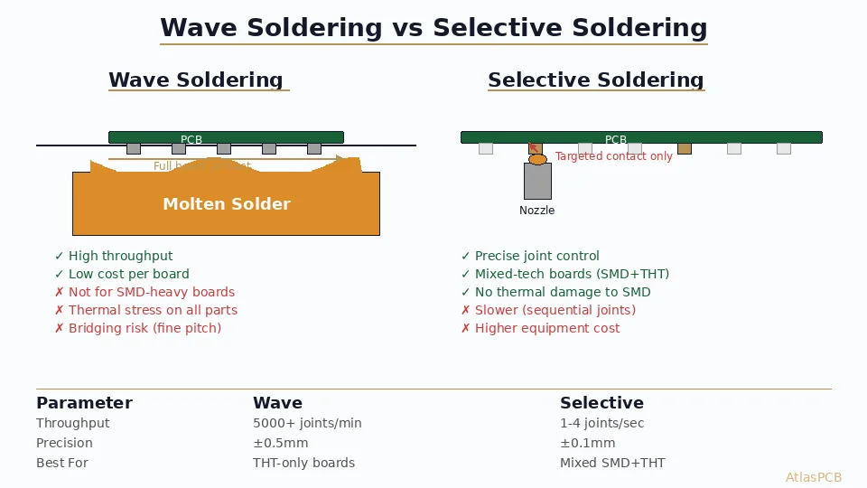
Wave soldering passes the entire bottom surface of a PCB assembly over a standing wave of molten solder. The board is conveyed through sequential process zones: fluxing, preheating, and finally contact with the solder wave itself. The flux activates oxide layers on the copper pads and component leads to promote wetting. Preheating drives off flux solvents and raises the board temperature gradually to reduce thermal shock when the assembly contacts the molten solder, which is maintained at approximately 250 to 260 degrees Celsius for SAC305 lead-free alloys.
The elegance of wave soldering lies in its simultaneous processing of all through-hole joints on the board in a single pass. A board with 200 through-hole solder joints requires no more time than a board with 20. This makes wave soldering extraordinarily efficient for boards with high through-hole component density, and its cycle time per board, typically 60 to 90 seconds depending on conveyor speed and preheat requirements, is essentially independent of joint count.
However, wave soldering in mixed-technology assemblies requires that all bottom-side SMT components be protected from contact with the solder wave. This is accomplished through selective pallets, also called wave solder carriers or fixtures, which mask the SMT components while exposing only the through-hole solder joints to the wave. These pallets are typically machined from Durostone or titanium and must be custom-designed for each PCB assembly. The pallet design must provide adequate clearance around SMT components to prevent contact damage while maintaining sufficient solder access to the through-hole joints.
In our production experience, wave solder pallet design is both an art and an engineering discipline. A pallet that provides generous clearance around tall SMT components may restrict solder access to nearby through-hole joints, creating insufficient fill or cold joints. Conversely, aggressive cutouts that maximize solder exposure can allow solder to wick under the pallet edge and bridge to adjacent SMT pads. We have refined our pallet design process through analysis of hundreds of assemblies to develop guidelines for minimum clearances, gasket channel placement, and thermal relief features that balance these competing requirements.
Selective Soldering: Precision at the Point of Need
Selective soldering takes the opposite philosophical approach. Rather than immersing the entire board bottom in solder and masking what should not be soldered, selective soldering applies solder only where it is needed, one joint or one group of joints at a time. The technology uses either a miniature solder fountain, which creates a small standing wave from a nozzle positioned beneath the specific through-hole joint, or a robotic solder iron tip for individual pin soldering.
Modern selective soldering systems typically employ a three-stage process. First, a programmable flux spray head applies flux precisely to the target solder joints using either a drop-jet or micro-spray nozzle. The flux application pattern is programmed for each joint or joint group, applying just enough flux to activate the surfaces without contaminating adjacent areas. Second, a bottom-side infrared or convection preheater raises the local board temperature. Third, the solder nozzle moves to each programmed position and dwells for a specified contact time, typically 2 to 5 seconds per joint or joint group, allowing solder to flow up through the barrel and create a complete fillet.
The elimination of the wave solder pallet is selective soldering’s most significant advantage for mixed-technology assemblies. With no pallet required, there is no fixture cost, no pallet storage requirement, and no thermal mass added to the assembly that would increase preheat time. For prototype quantities and low-volume production, the absence of pallet tooling cost can be decisive. A wave solder pallet typically costs between 3,000 and 8,000 USD depending on complexity, and modifications required by engineering changes add additional expense and lead time.
Thermal Profile Considerations
The thermal experience of the PCB assembly differs fundamentally between the two processes. In wave soldering, the entire board receives a uniform preheat profile as it traverses the preheat zone, then the full board bottom contacts the solder wave simultaneously. The board experiences a relatively uniform thermal profile, with the primary thermal gradient running from the top surface, which is cooler, through the board thickness to the bottom surface in contact with solder. This uniform heating is generally benign for most components, though heat-sensitive devices on the top side of thick boards may require special consideration.
Selective soldering creates a highly localized thermal event. The solder nozzle heats a small area of the board, typically a circle of 10 to 20 mm diameter depending on nozzle size and dwell time, to soldering temperature while the surrounding board remains relatively cool. This localized heating creates steep thermal gradients that can induce mechanical stress in the board and components. However, the total thermal energy input to the assembly is dramatically lower than wave soldering, which is advantageous for heat-sensitive assemblies or boards with components that have already undergone multiple reflow cycles.
From our process engineering data, we have measured peak board temperatures during selective soldering that are 30 to 50 degrees Celsius lower than wave soldering at locations 15 mm from the solder point. This reduced thermal exposure extends the remaining thermal budget for components that have already consumed significant solder reflow cycles, which is increasingly relevant for complex assemblies that undergo three or more reflow passes before through-hole soldering.
Defect Rate Analysis and Process Windows
The defect profiles of wave and selective soldering differ in character, though both can achieve excellent quality when properly controlled. Wave soldering defects are dominated by bridging between adjacent pins or pads, particularly for fine-pitch through-hole connectors with pin spacing below 2.0 mm. The solder wave contact angle, conveyor speed, board exit angle, and nitrogen inerting all influence bridge formation. In our production data, wave soldering of 0.1-inch pitch through-hole connectors achieves bridge defect rates below 50 ppm when all process parameters are optimized, but fine-pitch connectors at 1.27 mm spacing may exhibit bridge rates of 200 to 500 ppm without careful process tuning.
Selective soldering, by contrast, rarely produces bridges because the nozzle diameter and position are controlled for each joint. The primary defect mode for selective soldering is insufficient hole fill, which occurs when the dwell time, solder temperature, or flux activity is inadequate to achieve complete capillary flow through the barrel. Insufficient fill defects are particularly common in ground plane connections where the thermal mass of the connected copper plane draws heat away from the joint faster than the nozzle can supply it. We address this through zone-specific programming, where joints connected to heavy copper planes receive extended dwell times or elevated nozzle temperatures compared to isolated pins.
Another defect category unique to selective soldering is flux-related contamination. Because the flux spray system must accurately target each joint, any overspray onto adjacent SMT pads or component bodies can cause cosmetic defects or, in severe cases, dendritic growth under humid conditions. Modern selective soldering systems use vision-guided flux dispensing with droplet volumes as small as 2 nanoliters to minimize overspray, but the process validation must confirm adequate flux coverage on target pads without contamination of adjacent areas.
Cost Comparison Across Production Volumes
The economic comparison between wave and selective soldering is volume-dependent, and the crossover point depends on several factors specific to each assembly. Wave soldering has higher fixed costs due to the pallet tooling requirement, higher consumable costs from the larger solder pot that requires periodic alloy replenishment, and higher energy costs from maintaining a large molten solder reservoir. However, its per-board processing time is short and essentially fixed regardless of through-hole joint count.
Selective soldering has minimal fixed costs, no tooling requirement, and lower consumable usage, but its per-board processing time scales linearly with the number of through-hole joints. A board with 10 through-hole joints might require 45 seconds of selective soldering time, while a board with 100 joints might require 6 to 8 minutes. This linear scaling makes selective soldering increasingly expensive per board as joint count rises.
In our facility’s cost modeling, the crossover point typically occurs between 500 and 2,000 boards for a typical mixed-technology assembly with 30 to 50 through-hole joints. Below this volume, selective soldering is more economical because the pallet tooling cost cannot be amortized across enough boards. Above this volume, wave soldering’s faster cycle time and fixed per-board cost overcome the tooling amortization. However, this crossover shifts dramatically based on joint count, pallet complexity, and the engineering change frequency. Assemblies that undergo frequent revisions may never reach the wave soldering crossover because each revision requires a new or modified pallet.
Process Selection Methodology
The choice between wave and selective soldering should not be made solely on economic grounds. Several technical factors may dictate the selection regardless of cost optimization. If the board contains bottom-side SMT components that cannot tolerate the thermal exposure of wave soldering, even with a protective pallet, selective soldering becomes mandatory. If through-hole components are located in areas surrounded by tall SMT components that would make pallet design impractical, selective soldering avoids the geometric constraints. If the board has mixed-finish pads where some through-holes require standard soldering and others have been designated for press-fit insertion, selective soldering can target only the appropriate joints.
Conversely, wave soldering may be preferred when through-hole component density is very high, when the bottom side has minimal SMT population that is easily masked, or when production volumes are high enough to justify the tooling investment. Some assemblies benefit from a combination approach, where the majority of through-hole joints are wave soldered and a few problematic joints in thermally sensitive areas receive selective soldering as a secondary operation.
In our assembly operations, approximately 60 percent of mixed-technology builds now use selective soldering as the primary through-hole process, reflecting the industry trend toward higher-mix, lower-volume production with frequent engineering changes. The remaining 40 percent use wave soldering, primarily for established high-volume products where the tooling investment is justified and the assembly design is stable. We encourage customers to discuss their production volume forecasts and revision expectations early in the design phase so that the appropriate soldering technology can be factored into the DFM review, ensuring that through-hole component placement and spacing are optimized for the intended process.
Future Trends and Hybrid Approaches
The selective soldering technology continues to evolve toward higher throughput. Multi-nozzle systems with two or four independent soldering heads operating simultaneously can reduce cycle time proportionally, narrowing the economic gap with wave soldering. Some advanced systems now offer miniature wave modules that can process an entire connector row in a single pass, combining the speed advantage of wave contact with the selectivity of programmed positioning.
Meanwhile, wave soldering systems have incorporated programmable electromagnetic pump control that shapes the wave profile dynamically as the board passes overhead, effectively creating a hybrid between traditional wave and selective approaches. These variable-geometry wave systems can reduce the wave contact area for sensitive regions of the board while maintaining full-width contact for dense through-hole areas.
The fundamental engineering challenge remains unchanged regardless of which technology is employed: achieving complete solder fill in plated through-holes while avoiding thermal damage to surrounding components and maintaining zero-defect quality expectations. Both wave and selective soldering can meet this challenge when the process is matched to the assembly design and production requirements, and the manufacturer has the expertise and process control systems to maintain consistent quality across production volumes.
About AtlasPCB — We specialize in complex PCB manufacturing for HDI, RF, and high-reliability applications. Explore our PCB assembly services, or get an free engineering DFM review . Every order includes free engineering review. Get your quote.
Reviewed by AtlasPCB Engineering Team — IPC-certified manufacturing specialists with 15+ years of production experience in HDI, RF, and high-reliability PCB fabrication. Content based on factory floor data and real customer design reviews.
- Selective Soldering
- Wave Soldering
- PCB Assembly
- Through-Hole
- DFM