· AtlasPCB Engineering Team · Engineering · 17 min read
Rigid-Flex PCB Manufacturing: The Engineer's Complete Guide to Design, Material Selection, and Ordering from China
A comprehensive guide to rigid-flex PCB design and manufacturing — covering stackup fundamentals, bend zone rules, material selection, DFM pitfalls, and how to evaluate manufacturers. Written by a rigid-flex manufacturer with real cost data and engineering insight.
Quick Answer
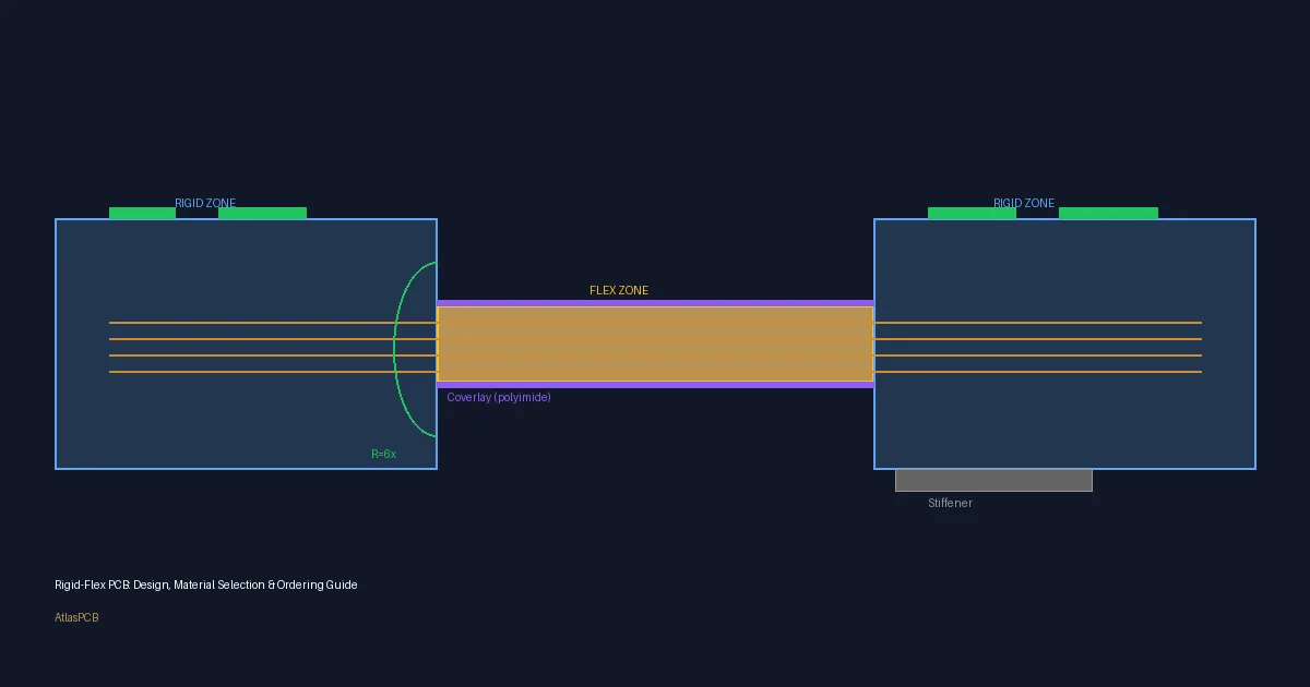
Rigid-flex PCBs combine rigid FR-4 sections with flexible polyimide sections in a single laminated structure, eliminating connectors and enabling 3D packaging. Successful rigid-flex manufacturing requires careful stackup design (flex layers typically on inner layers for static applications), proper bend zone rules (minimum bend radius of 6x total flex thickness for static, 12x for dynamic), and selection between adhesive-based and adhesiveless polyimide constructions based on reliability requirements.
When Rigid-Flex Actually Makes Sense
The decision to use rigid-flex construction should never be driven by novelty or the assumption that “newer is better.” Rigid-flex PCBs serve a specific engineering purpose: they eliminate board-to-board connectors and flex cables in applications where those interconnects create unacceptable reliability risk, consume too much space, or add assembly complexity that outweighs the cost premium.
The crossover point where rigid-flex becomes economically justified typically occurs when a design requires three or more flex cable connections between rigid sections, when the available volume envelope cannot accommodate connector heights, or when the application demands vibration resistance that crimped connectors cannot guarantee. In aerospace and medical implantable devices, the reliability imperative alone justifies rigid-flex regardless of cost. In consumer electronics, the space savings typically need to reduce overall system volume by at least 15-20% to justify the 3-8x cost premium over discrete rigid boards with flex cables.
From our production experience, approximately 40% of rigid-flex inquiries we receive would actually be better served by separate rigid boards connected with flat flex cables. We tell those customers directly — it saves them money and gives us credibility when we recommend rigid-flex for applications that genuinely need it.
Reviewed by AtlasPCB Engineering Team
Rigid-Flex Stackup Design Fundamentals
The stackup is where rigid-flex design either succeeds or fails. Unlike standard rigid PCBs where the stackup primarily affects impedance and signal integrity, a rigid-flex stackup directly determines mechanical reliability, bend performance, and manufacturing yield. Getting this wrong is the single most common reason rigid-flex projects require costly redesigns.
Flex Layer Placement
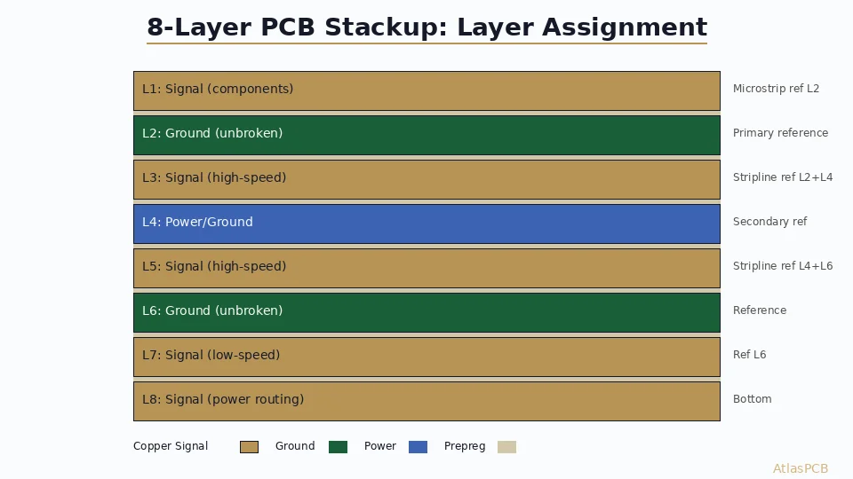
The most fundamental stackup decision is where to place flex layers within the overall layer structure. For static flex applications (the board bends once during assembly and remains in position), flex layers are typically placed on inner layers of the stackup. This shields the flex copper from external mechanical stress and allows rigid outer layers to carry components on both sides of the rigid sections.
For dynamic flex applications (the board bends repeatedly during product operation, such as a laptop hinge or printer head), flex layers must be placed at or near the neutral axis of the flex section to minimize strain on copper conductors. When only one or two flex layers are needed for signal routing, centering them within the flex zone’s cross-section distributes bending stress equally between the inner and outer surfaces.
A critical subtlety that many designers miss: in the rigid sections, the flex layers are fully laminated with the surrounding rigid layers and behave as standard innerlayers. The “flex” property only matters in the flex zones where the rigid materials are absent. This means your flex layers must satisfy both flex-zone bend requirements AND rigid-zone impedance/routing requirements — two potentially conflicting constraints that require careful dielectric thickness planning.
Adhesive-Based vs Adhesiveless Construction
This material choice has profound implications for reliability, cost, and manufacturing complexity. Adhesive-based flex constructions use an acrylic or epoxy adhesive layer (typically 25μm) to bond copper foil to the polyimide substrate. Adhesiveless constructions deposit copper directly onto the polyimide through sputtering and electroplating, eliminating the adhesive entirely.
Adhesive-based materials (Dupont Pyralux LF series, Shengyi SF305C) are less expensive, easier to process, and adequate for static flex applications with operating temperatures below 130°C. However, the acrylic adhesive has a significantly higher coefficient of thermal expansion than either copper or polyimide, creating differential stress during thermal cycling that can initiate delamination after 200-500 cycles depending on layer count.
Adhesiveless materials (Dupont AP series, Shengyi SF305HG) cost 30-40% more but provide dramatically superior thermal cycling resistance (1000+ cycles), tighter dimensional stability for fine-pitch features, and better chemical resistance. For any application involving lead-free reflow (peak temperatures above 250°C), automotive operating environments (-40°C to +125°C), or dynamic flex with more than 10,000 bend cycles, adhesiveless construction is not optional — it is the minimum acceptable specification.
In our facility, approximately 65% of rigid-flex orders now specify adhesiveless materials, up from roughly 40% three years ago. The shift reflects both increasing reliability demands and the growing adoption of lead-free assembly processes that stress adhesive-based constructions beyond their thermal limits.
Coverlay vs Photoimageable Solder Mask
In flex zones, the standard liquid photoimageable (LPI) solder mask used on rigid sections is inappropriate. LPI is brittle — it cracks when bent, exposing copper to corrosion and potentially creating short circuits from cracked mask fragments. Flex zones require coverlay: a pre-formed polyimide film (typically 25μm polyimide + 25μm adhesive) that is die-cut to shape and laminated over the flex copper.
Coverlay provides excellent flex endurance but has a significant limitation: it cannot be patterned to the same resolution as LPI solder mask. Minimum coverlay opening dimensions are typically 200μm (8 mil), compared to 75μm (3 mil) for LPI. This constrains component placement in flex zones — another reason why components should only be placed on rigid sections.
For rigid-to-flex transition zones where fine pad access is needed near the flex boundary, some manufacturers offer photoimageable coverlay (PIC) materials. These combine the flexibility of coverlay with the patterning precision of photoimaging, but add approximately 20% to flex-zone processing cost. We recommend PIC only when standard coverlay openings cannot meet pad access requirements within 2mm of the rigid-flex boundary.
RIGID-FLEX DESIGN REVIEW
Unsure About Your Stackup?
Upload your stackup drawing and our engineers will review layer assignments, material compatibility, and bend zone feasibility within 24 hours.
Upload Design ›
Critical Design Rules for Bend Zones
Bend zone design is where rigid-flex differs most dramatically from standard PCB layout. The flex zone is not simply “a rigid board that happens to be thin” — it is a mechanical structure subject to repeated or sustained bending stress that will fatigue and crack copper conductors if design rules are violated.
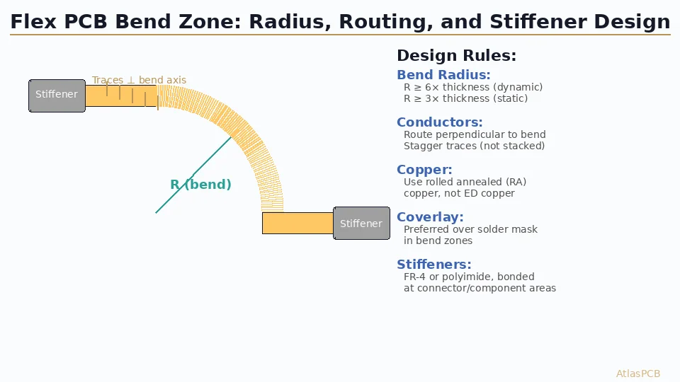
Minimum Bend Radius
The minimum allowable bend radius depends on the total flex thickness, the number of copper layers in the flex zone, copper type, and whether the application is static or dynamic. The fundamental rule uses total flex section thickness (including all copper layers, polyimide, adhesive, and coverlay) as the reference dimension.
For single-sided flex (one copper layer): static minimum is 3x total thickness, dynamic minimum is 6x. For double-sided flex (two copper layers): static minimum is 6x, dynamic minimum is 12x. For four-layer flex sections: static minimum is 12x, dynamic minimum is 25x. These ratios ensure that copper strain at the outer surface remains below the fatigue threshold that initiates microcracking.
A practical example: a double-sided flex section with 0.2mm total thickness requires minimum 1.2mm static bend radius (adequate for a fold-over-once installation) or 2.4mm dynamic bend radius (adequate for a repeated-hinge application). Violating these minimums by even 20% can reduce flex life from millions of cycles to hundreds — a catastrophic reliability failure that may not appear in prototype testing but manifests in field returns.
Copper Type Matters
Electrodeposited (ED) copper has a columnar grain structure that is inherently less ductile than rolled annealed (RA) copper. For flex zones subject to any bending, RA copper is strongly preferred. The elongation at break for RA copper is typically 20-30%, compared to 8-12% for ED copper. This difference directly translates to flex life — RA copper flex circuits typically survive 5-10x more bend cycles than equivalent ED copper designs.
However, RA copper is not universally available in all thicknesses and not all manufacturers stock it. When specifying your design, explicitly call out “rolled annealed copper in flex zones” on your fabrication drawing. If your manufacturer cannot provide RA copper, you must increase bend radius minimums by 50% to compensate for ED copper’s reduced ductility.
Trace Routing in Bend Zones
Route all traces perpendicular to the bend axis. Never route traces parallel to the bend — parallel traces experience concentrated strain along their entire length, while perpendicular traces distribute strain across their width. A trace running parallel to the bend axis can crack after as few as 100 cycles, while the same trace routed perpendicular to the bend survives indefinitely under the same conditions.
When trace direction must transition from one orientation to another, make that transition in the rigid section — never change routing direction within the flex zone. Additionally, stagger traces on multi-layer flex sections rather than stacking them directly above/below each other. Stacked traces create localized stress concentration that promotes delamination between layers during bending.
Trace width in flex zones should be wider than the minimum required by impedance targets. We recommend minimum 100μm (4 mil) traces in flex zones even when the rigid zones use 75μm (3 mil). The wider trace provides more cross-sectional copper area to resist fatigue cracking and distributes strain over a larger surface.
The 7 Most Common Rigid-Flex DFM Failures
After reviewing thousands of rigid-flex designs over the past decade, we have identified the recurring DFM issues that cause orders to be rejected or require redesign. These failures share a common root cause: engineers designing rigid-flex boards as if they were standard rigid PCBs, without accounting for the unique mechanical and manufacturing constraints of flex zones and transitions.
Failure 1: Copper cracking at rigid-flex transitions. The transition zone where rigid laminate ends and flex begins is the highest-stress region of the entire board. Without proper design attention, copper traces crack at this boundary within weeks of installation. The fix is tear-drop shaped pad entries at transition boundaries, copper anchoring tabs that extend 0.5mm into the rigid zone, and gradual thickness transitions rather than abrupt steps.
Failure 2: Vias placed in or too close to flex zones. Any via placed within a flex zone creates a rigid stress concentration point that cannot bend with the surrounding material. This invariably causes cracking, delamination, or barrel fracture. Maintain minimum 1.0mm clearance between any via and the start of the flex zone. For dynamic flex, increase this to 2.5mm.
Failure 3: Coverlay opening dimensions too small. Designers accustomed to LPI solder mask specify coverlay openings at 75-100μm clearance around pads. Coverlay registration tolerance is approximately 150μm (6 mil) in production — far looser than LPI. Design coverlay openings with minimum 250μm (10 mil) clearance around pads to prevent coverlay from covering exposed copper that requires soldering.
Failure 4: Traces routed parallel to the bend axis. As discussed in the bend zone section, this is the single most common routing violation we see in rigid-flex designs. It typically appears when a designer auto-routes the board and the router optimizes for length rather than flex reliability. Always verify trace direction in flex zones after routing is complete.
Failure 5: Asymmetric copper distribution in flex zones. When one side of a flex section has significantly more copper coverage than the other, bending creates unequal strain distribution that causes the high-copper side to experience compressive stress while the low-copper side experiences tensile stress. The result is accelerated fatigue on the tensile side. Balance copper coverage between layers in flex zones to within 20% of each other.
Failure 6: Wrong material specification. Specifying adhesive-based flex material for a dynamic application, or specifying ED copper when RA is required, creates reliability time bombs that pass initial testing but fail in the field. Always explicitly specify: polyimide type (adhesive/adhesiveless), copper type (RA/ED), coverlay type, and stiffener material on your fabrication drawing.
Failure 7: Insufficient rigid-to-flex overlap. The rigid laminate must overlap the flex section by at least 1.0mm (preferably 1.5-2.0mm) at each transition. Insufficient overlap provides inadequate mechanical anchoring, allowing flex layers to peel away from the rigid section under repeated thermal cycling or mechanical stress.
FREE DFM REVIEW
Catch These Failures Before Production
Our engineering team identifies rigid-flex DFM issues in your Gerber files before fabrication begins — preventing costly redesigns.
Submit for Review ›Material Selection Guide
Choosing the right materials for rigid-flex construction requires balancing performance requirements against cost and availability. The material stack in a rigid-flex board is substantially more complex than a standard rigid PCB — you are combining two fundamentally different material systems (FR-4 and polyimide) that must survive lamination together and function reliably as a unified structure.
Polyimide Film Selection
The base polyimide film forms the dielectric substrate of flex zones. Standard film thickness options are 12.5μm, 25μm, and 50μm. For most applications, 25μm provides the optimal balance between flexibility (thinner is more flexible) and mechanical robustness (thicker resists tearing and puncture). Use 12.5μm only when bend radius is extremely tight and signal count is low; use 50μm when flex zones must span distances exceeding 100mm where unsupported film sag is a concern.
The industry-standard film is Kapton (Dupont trademark), but equivalent films from Kaneka, SKC, and UBE are mechanically and electrically interchangeable at lower cost. When specifying polyimide, the critical electrical parameter is dielectric constant — standard polyimide runs 3.2-3.4 at 1 GHz, which is lower than FR-4 (4.2-4.5) and creates impedance discontinuities at rigid-flex transitions unless the stackup accounts for this difference.
Bondply and Prepreg for Rigid-Flex Lamination
Bonding the rigid sections to the flex core requires specialized bondply (also called “bonding sheet” or “no-flow prepreg”). Standard high-flow prepreg used in rigid PCB lamination can flow into flex zones during press, contaminating exposed flex copper or creating resin dams that restrict bending. Low-flow or no-flow bondply specifically designed for rigid-flex construction prevents this by gelling quickly during lamination without excessive flow.
The bonding sheet must be die-cut to stop precisely at the rigid-flex boundary. Registration accuracy of this die-cut directly affects transition zone quality — misalignment greater than 200μm can create exposed adhesive edges that attract contamination or weak bondlines that delaminate under thermal stress.
Stiffener Selection
Stiffeners are rigid material pieces bonded to specific areas of flex zones where components are mounted or where connector insertion force requires structural support. Common stiffener materials include FR-4 (cheapest, adequate for most applications), polyimide (lighter weight, matches CTE of flex), and stainless steel or aluminum (highest stiffness-to-thickness ratio, used for thin sections requiring maximum rigidity).
Stiffener thickness is typically 0.2-1.0mm depending on rigidity requirements. Bond them with pressure-sensitive adhesive (PSA) for non-soldering applications, or thermally-cured adhesive for components that will experience reflow temperatures. Always specify stiffener locations on your fabrication drawing — missing stiffener callouts is a common oversight that delays production by 3-5 days while the manufacturer requests clarification.
How to Get an Accurate Rigid-Flex Quote
Quoting rigid-flex PCBs takes substantially longer than rigid boards — typically 2-3 business days versus same-day for standard rigid. This delay exists because rigid-flex quoting requires engineering review of mechanical feasibility, material compatibility, and manufacturing sequence planning. Providing complete documentation upfront eliminates back-and-forth and accelerates quoting to 1-2 days.
Required Documentation
Beyond standard Gerbers and drill files that every PCB order requires, rigid-flex quotes need these additional documents:
A detailed stackup drawing showing which layers are rigid-only, which are flex-only, and which continue through both zones. Indicate material type, copper weight, and dielectric thickness for each layer. Specify adhesive-based or adhesiveless construction explicitly.
A mechanical drawing showing the board outline including all rigid and flex zones clearly dimensioned. Include bend radius callouts, flex zone lengths, and rigid-to-flex overlap dimensions. Indicate whether each flex zone is static or dynamic.
Material specification notes: polyimide type, copper type (RA vs ED), coverlay material and thickness, stiffener material and locations, and any specific impedance requirements in flex zones.
Red Flags When Evaluating Manufacturers
If a manufacturer quotes your rigid-flex board without asking any clarifying questions about the flex zones, bend requirements, or material preferences, that is a significant warning sign. Rigid-flex is complex enough that a competent manufacturer will always have technical questions during quoting — it means they are actually reviewing your design for manufacturability rather than simply pricing by layer count and area.
Similarly, be cautious of manufacturers who claim identical lead times for rigid-flex and standard rigid boards. Rigid-flex requires sequential lamination, specialized flex material handling, and additional quality inspection steps that add 5-10 days to production time compared to equivalent-layer-count rigid boards.
READY TO QUOTE
Get Your Rigid-Flex Quote in 48 Hours
Upload your Gerbers + stackup drawing. Our engineers review feasibility and provide detailed pricing within 2 business days.
Get Quote ›What to Look for in a Rigid-Flex Manufacturer
Not every PCB manufacturer that claims rigid-flex capability actually produces it reliably at scale. Rigid-flex requires specialized equipment (vacuum lamination presses, laser drills, controlled-depth routing), trained process engineers, and quality systems beyond standard rigid PCB production. Here is how to evaluate whether a manufacturer’s rigid-flex claims are genuine.
Essential Equipment
Vacuum lamination press capability is non-negotiable for rigid-flex. Standard hydraulic presses used for rigid PCB lamination cannot achieve the void-free bondlines required in rigid-flex transition zones. Vacuum lamination removes trapped air during the press cycle, preventing delamination at the rigid-flex interface. Ask your potential manufacturer specifically whether they have vacuum lamination — not just “lamination capability.”
Controlled-depth routing (also called Z-axis routing or depth-controlled milling) is required to create the rigid-to-flex transitions. The router must cut through the rigid laminate layers while stopping precisely at the flex layers without damaging them. Depth accuracy of plus or minus 50μm is required; anything worse risks cutting into flex copper or leaving residual rigid material that prevents proper bending.
Certifications That Matter
For rigid-flex, the relevant IPC standard is IPC-6013 (Qualification and Performance Specification for Flexible/Rigid-Flexible Printed Boards). This is separate from IPC-6012 which covers rigid boards. A manufacturer certified to IPC-6012 is not necessarily qualified for rigid-flex — verify IPC-6013 compliance specifically.
For medical or aerospace applications, ask for cross-section photomicrographs of rigid-flex transition zones from recent production. These images reveal lamination quality, copper condition at transitions, and adhesive flow control better than any certification document.
Our Rigid-Flex Capabilities
AtlasPCB fabricates rigid-flex assemblies from 4 to 22 layers with up to 6 flex-to-rigid transitions per board. Our facility processes both adhesive-based and adhesiveless polyimide constructions, using vacuum autoclave lamination for void-free bondlines and controlled-depth routing with plus or minus 25μm accuracy for clean rigid-flex transitions.
Our standard rigid-flex capabilities include minimum 75μm trace and space in rigid zones, minimum 100μm in flex zones, RA copper in all flex layers, and coverlay openings to 200μm minimum. We support IPC-6013 Class 2 and Class 3 quality requirements for commercial and high-reliability applications.
Typical lead times: prototype (5-10 panels) in 12-18 working days, production quantities (50+ panels) in 15-22 working days. Rush service available for prototype quantities with 8-12 day turnaround at premium pricing.
ATLASPCB
Start Your Rigid-Flex Project
From stackup review through production delivery. Upload your design files and get engineering feedback within 48 hours.
Upload Gerbers ›
Reviewed by AtlasPCB Engineering Team
Related Reading:
About AtlasPCB — We specialize in complex PCB manufacturing for HDI, RF, and high-reliability applications. Explore our rigid-flex PCB manufacturing, free engineering DFM review, or get an full PCB manufacturing capabilities . Every order includes free engineering review. Get your quote.
Reviewed by AtlasPCB Engineering Team — IPC-certified manufacturing specialists with 15+ years of production experience in HDI, RF, and high-reliability PCB fabrication. Content based on factory floor data and real customer design reviews.
Frequently Asked Questions
What is the minimum bend radius for a rigid-flex PCB?
How much does a rigid-flex PCB cost compared to rigid boards?
What files do I need to provide for a rigid-flex PCB quote?
Should I use adhesive-based or adhesiveless polyimide for rigid-flex?
- rigid-flex PCB
- PCB manufacturer
- DFM
- polyimide
- flex design
- PCB ordering guide
- IPC-6013