· AtlasPCB Engineering Team · Engineering · 14 min read
PCB Surface Preparation Methods Compared: Micro-Etch Chemistry, Roughness Profiles, and Their Impact on Adhesion and Signal Integrity
Selecting between sodium persulfate, hydrogen peroxide sulfuric acid, and cupric chloride micro-etch systems requires balancing copper adhesion strength above 6 lb/in against surface roughness below 0.5 micrometers Rz for high-speed signal performance.
The Fundamental Role of Surface Preparation in PCB Manufacturing
Surface preparation occurs at multiple stages throughout the PCB manufacturing process, and each instance serves a specific purpose critical to the final product quality. Before photoresist lamination, the copper surface must be clean and uniformly micro-roughened to ensure photoresist adhesion during developing and plating. Before inner layer oxide treatment, surfaces require specific roughness profiles to promote mechanical interlocking with the oxide crystals. Before solder mask application, outer layer copper must present a controlled surface energy for LPI coating adhesion. Each of these preparation steps uses chemical micro-etching to create a specific surface topography, and the choice of micro-etch chemistry directly determines the roughness profile, copper removal rate, and ultimate adhesion performance.
At our manufacturing facility, we run 7 distinct surface preparation steps across the full multilayer PCB process flow, each using chemistry optimized for its specific function. The total copper removed by micro-etching across all process steps amounts to 3 to 8 micrometers per surface, which must be accounted for in the original copper thickness specification. A 1-ounce (35 micrometer) copper layer that passes through 4 micro-etch steps at 1.5 micrometers removal each loses 6 micrometers total, reducing the effective final thickness to 29 micrometers. This 17 percent reduction is significant for current-carrying capacity calculations and must be included in the design phase trace width determination. IPC-6012 Section 3.5.3 specifies minimum conductor thickness after processing, making micro-etch copper removal a critical manufacturing variable to control.
Sodium Persulfate: The Traditional Micro-Etch Chemistry
Sodium persulfate (Na2S2O8) has served as the baseline micro-etch chemistry in PCB manufacturing since the 1970s. Operating at concentrations of 100 to 200 grams per liter at temperatures of 30 to 40 degrees Celsius, sodium persulfate dissolves copper through an oxidation reaction that produces copper sulfate as the primary byproduct. The etch rate at standard operating conditions ranges from 0.8 to 1.5 micrometers per minute, providing predictable copper removal with processing times of 60 to 120 seconds for the typical 1.0 to 2.0 micrometer removal target.
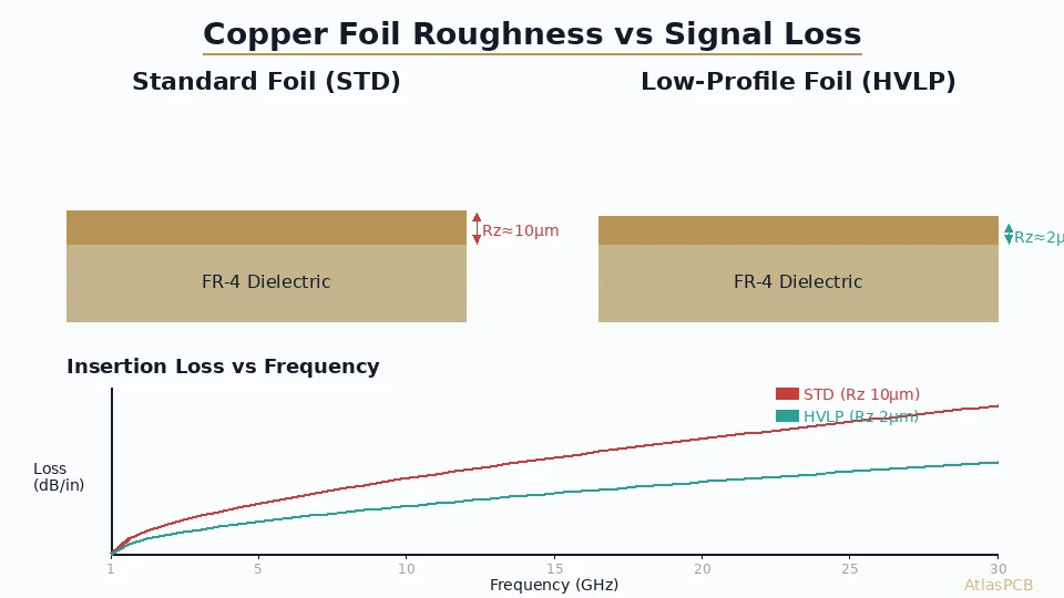
The surface profile created by sodium persulfate etching is characterized by broad, shallow pitting with peak-to-valley roughness (Rz) of 1.0 to 2.5 micrometers. This relatively aggressive roughness profile provides excellent mechanical adhesion for subsequent coating steps, with peel strength values of 6 to 9 pounds per inch (lb/in) for photoresist on treated surfaces. However, the same roughness that promotes adhesion increases conductor losses at high frequencies. The Hammerstad-Jensen model and more recent Huray snowball model both demonstrate that surface roughness increases effective conductor resistance proportional to the ratio of roughness height to skin depth. At 10 GHz where copper skin depth is approximately 0.66 micrometers, a surface roughness Rz of 2.0 micrometers increases conductor loss by 40 to 60 percent compared to a perfectly smooth surface. This loss penalty makes sodium persulfate inappropriate for signal layers in designs operating above 10 Gbps.
Hydrogen Peroxide Sulfuric Acid: Controlled Roughness for High-Speed Applications
The hydrogen peroxide sulfuric acid (H2O2/H2SO4) micro-etch system offers significantly finer surface roughness control compared to persulfate chemistry. Operating at 2 to 5 percent H2O2 and 3 to 8 percent H2SO4 by volume at 25 to 35 degrees Celsius, this chemistry creates a uniform micro-crystalline copper surface with Rz values of 0.3 to 1.2 micrometers depending on process time and temperature. The lower roughness profile reduces high-frequency conductor losses by 25 to 40 percent compared to persulfate-treated surfaces while maintaining adequate adhesion (4 to 7 lb/in peel strength) for most PCB applications.
The chemistry operates through a catalytic cycle where H2O2 oxidizes metallic copper to Cu2+ ions, which then dissolve in the sulfuric acid solution. Unlike persulfate which is consumed stoichiometrically, the peroxide system can be continuously replenished by adding H2O2, with copper dissolved accumulating in solution until it reaches a saturation limit of approximately 30 to 40 grams per liter. At our facility, we operate two peroxide-sulfuric micro-etch lines: one at conservative settings (Rz target 1.0 micrometer) for standard multilayer production, and one at aggressive settings (Rz target 0.5 micrometer) specifically for high-speed designs above 25 Gbps. The low-roughness line uses reduced H2O2 concentration (2 percent), lower temperature (25 degrees), and shorter immersion time (30 seconds) to achieve the fine surface texture needed for Megtron 6, Panasonic M7NE, and similar very-low-loss laminate systems where the manufacturer specifies surface roughness below 0.8 micrometer Rz for optimal bonding.
Cupric Chloride and Ferric Chloride: High-Speed Etch Alternatives
Cupric chloride (CuCl2) micro-etch chemistry provides unique surface morphology characteristics not achievable with persulfate or peroxide systems. The chloride-based attack creates a needle-like micro-structure on the copper surface, with extremely fine asperities measuring 0.1 to 0.5 micrometers in height and 0.05 to 0.2 micrometers in width. This fine-needle topography provides high specific surface area for chemical bonding while maintaining low effective roughness as “seen” by high-frequency electromagnetic fields. The reason is that surface features smaller than one-third of the skin depth at the operating frequency contribute minimally to RF loss while still providing mechanical anchoring for subsequent coatings.
Ferric chloride (FeCl3) micro-etch operates similarly but with different selectivity characteristics. At concentrations of 30 to 50 grams per liter iron (as Fe3+) in hydrochloric acid solution, ferric chloride produces etch rates of 1.0 to 2.0 micrometers per minute with surface roughness profiles between persulfate and peroxide systems (Rz of 0.8 to 1.8 micrometers). The primary advantage of chloride-based micro-etching is consistent etch rate independent of dissolved copper concentration up to 100 grams per liter, providing more stable processing in high-volume production environments. MEC Corporation (Japan) and Atotech (Germany) both offer proprietary chloride-based micro-etch formulations specifically optimized for inner layer adhesion promotion, with MEC’s etchBOND CZ-8101 claiming Rz control within plus or minus 0.2 micrometers across production bath life.
Adhesion Promotion for Inner Layers: Oxide vs Alternative Treatments
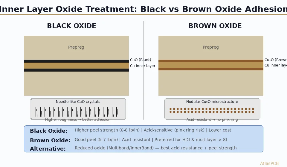
Inner layer adhesion treatment represents the most critical surface preparation step for multilayer PCB reliability. The traditional approach uses black oxide (CuO) or brown oxide (reduced CuO) to create a conversion coating on copper surfaces before lamination. Black oxide forms needle-like crystals 2 to 5 micrometers tall that provide massive surface area for mechanical interlocking with flowing prepreg resin during lamination. The IPC-4562 standard specifies minimum oxide weight of 0.25 to 0.40 mg/cm2 for adequate adhesion, typically requiring 2 to 4 minutes immersion in the oxide bath at 70 to 85 degrees Celsius.
However, black oxide crystals are brittle and susceptible to “pink ring” defects around drilled holes where acidic drilling coolant or desmear chemicals dissolve the oxide layer, exposing bare copper that appears as a pink halo visible in transmitted light inspection. Alternative oxide treatments address this vulnerability through various approaches. MacDermid Enthone’s M-Bond and Atotech’s BondFilm create modified oxide coatings with improved acid resistance. MEC’s CZ-8100 series applies an organo-metallic conversion coating that provides equivalent adhesion (5 to 8 lb/in peel strength per IPC-TM-650 method 2.4.8) without the crystalline structure susceptible to pink ring. In our production line, we transitioned from traditional black oxide to a reduced brown oxide process (MEC CZ-8101) in 2024, reducing pink ring defect rates from 2.3 percent to 0.1 percent of drilled panels while maintaining inner layer peel strength above 6 lb/in. The process operates at 30 degrees Celsius (versus 80 degrees for traditional oxide), saving significant energy costs while improving environmental sustainability.
Measuring Surface Roughness: Profilometry and Its Limitations
Quantifying micro-etch surface roughness requires appropriate measurement techniques matched to the relevant scale. Contact profilometry using a stylus instrument (such as the Mitutoyo SJ-410) traces a diamond-tipped probe across the surface, recording height variations with vertical resolution of 0.01 micrometers. Standard roughness parameters reported include Ra (arithmetic mean deviation), Rz (ten-point height), and Rq (root mean square roughness). For PCB micro-etch qualification, Rz is the most commonly specified parameter because it captures peak-to-valley excursions that most directly correlate with both adhesion performance and signal loss.
However, contact profilometry samples only a single line across the surface, potentially missing variations in the perpendicular direction and certainly missing sub-micrometer features below the stylus tip radius (typically 2 to 5 micrometers). Optical methods including confocal microscopy and white light interferometry provide areal roughness data (Sa, Sz parameters per ISO 25178) with lateral resolution below 0.5 micrometers, capturing the full three-dimensional surface texture. For correlation with high-frequency signal loss, the most relevant metric is the Huray model’s tile area ratio, which describes the copper surface as a collection of hemispherical “snowballs” with a specific radius and density. This model, developed by Paul Huray at the University of South Carolina, provides the most accurate prediction of frequency-dependent conductor loss from 1 to 50 GHz. At our facility, we use both contact profilometry (Rz measurement, 3 readings per panel) for process control and SEM imaging at 5000x magnification for detailed morphology characterization when qualifying new micro-etch chemistries.
The Adhesion-Loss Trade-Off: Optimizing for Your Application
The fundamental engineering challenge in surface preparation is that adhesion strength and signal loss scale in opposite directions with increasing roughness. Higher roughness creates more mechanical interlock and greater adhesion force, but also increases conductor loss through the skin effect proximity mechanism. For a typical production line running mixed product types, the question becomes: what roughness target provides acceptable adhesion without excessive loss for the highest-speed signals in the design?
For designs operating below 5 GHz (equivalent to approximately 10 Gbps NRZ signaling), surface roughness has minimal impact on signal integrity, and maximum adhesion should be the optimization target. Rz values of 1.5 to 2.5 micrometers (achieved with persulfate micro-etch) provide peel strength above 7 lb/in with negligible frequency-dependent loss increase. For designs at 10 to 28 Gbps, the balance shifts toward moderate roughness (Rz 0.8 to 1.2 micrometers), accepting slightly lower adhesion of 5 to 6 lb/in in exchange for 20 to 30 percent lower conductor loss. For cutting-edge designs above 56 Gbps PAM4 where every 0.5 dB of channel margin matters, roughness must be controlled below Rz 0.5 micrometers, with adhesion ensured through chemical bonding mechanisms rather than mechanical interlock.
The emerging solution for ultra-high-speed applications uses “smooth copper” foils (HVLP or HVLP4 grades per IPC-4562A) with surface roughness below Rz 0.4 micrometers, combined with organo-silane or thiol-based adhesion promoters that create covalent bonds between copper and resin without requiring surface roughness. Mitsui Mining’s TQ-M9 and Circuit Foil’s HYF foils provide pre-manufactured smooth surfaces, while post-etch chemical treatments from Shikoku Chemicals (GLOSSA series) restore bonding capability after any copper surface processing that might have altered the original foil texture.
Process Control: Maintaining Micro-Etch Consistency in Production
Maintaining consistent micro-etch performance across thousands of panels requires careful monitoring of chemistry concentration, temperature, etch rate, and surface quality. The primary control parameter is copper removal rate, measured by weighing a standardized copper coupon before and after immersion for a fixed time (typically 60 seconds). The target removal rate depends on the specific application: 1.0 plus or minus 0.3 micrometers per minute for standard adhesion promotion, or 0.5 plus or minus 0.2 micrometers per minute for low-roughness high-speed processing.
For persulfate systems, concentration monitoring uses specific gravity measurement (target 1.05 to 1.15 g/ml) or redox titration. Dissolved copper buildup above 15 grams per liter reduces etch rate and changes surface morphology, requiring partial bath dump and refresh. For peroxide-sulfuric systems, both H2O2 concentration (measured by permanganate titration or automated sensors) and H2SO4 concentration (measured by acid-base titration) require independent monitoring at 4 to 8 hour intervals. Our horizontal conveyorized micro-etch lines include inline ORP (oxidation-reduction potential) sensors that provide continuous indirect measurement of peroxide concentration, triggering automatic dosing when ORP drops below the setpoint of 480 plus or minus 20 mV. This automation maintains etch rate within plus or minus 15 percent of target between manual titration checks, reducing the risk of over-etch or under-etch that would compromise either adhesion or surface roughness specifications.
Impact on Specific Manufacturing Steps: Resist, Solder Mask, and Wire Bonding
Each downstream process has unique surface preparation requirements that drive different micro-etch specifications. Dry film photoresist (such as DuPont Riston or Hitachi Chemical RY-3525) requires surface roughness of Rz 1.0 to 2.0 micrometers for reliable adhesion during alkaline developing, where the developer solution attempts to undercut the resist at pattern edges. Insufficient roughness causes resist lifting during development, creating ragged trace edges and potential short circuits from copper that was not protected during etching.
Solder mask (LPI type per IPC-SM-840) requires slightly different surface preparation: roughness of Rz 0.8 to 1.5 micrometers with emphasis on surface cleanliness (absence of oxidation and organic contamination) rather than purely mechanical roughness. The photoimageable mask cures by UV crosslinking and relies partially on chemical adhesion through epoxy-to-copper bonding, meaning the surface must be chemically active (free of oxide above 3 angstroms thickness) at the time of coating. This requires micro-etching immediately before mask application, with a maximum delay of 4 hours between preparation and coating in climate-controlled environments (below 50 percent RH).
For wire bonding applications (used in chip-on-board assemblies and specialized ENEPIG finishes), surface roughness requirements are inverted: the bonding surface must be as smooth as possible (Ra below 0.1 micrometers) to ensure uniform bond pad surface energy for consistent gold or aluminum wire wedge bonding. Micro-etching before ENEPIG plating must therefore be the gentlest possible treatment that provides adequate cleanliness without creating roughness that translates through the thin nickel-palladium-gold finish. We specify a maximum 15-second immersion in dilute peroxide-sulfuric (1.5 percent H2O2) for wire bond pad areas, removing only surface oxides without creating measurable roughness increase.
Environmental and Safety Considerations in Micro-Etch Chemistry
The chemical systems used for PCB micro-etching present varying environmental and workplace safety challenges that influence selection for new production lines. Sodium persulfate is classified as an oxidizer (GHS Category 1) that generates ammonium sulfate and copper sulfate waste streams requiring treatment before discharge. The spent solution contains 15 to 30 grams per liter dissolved copper, which must be reduced below 1 mg/l for wastewater discharge per EPA Clean Water Act guidelines (or equivalent local regulations). Standard treatment uses sulfide precipitation or electrowinning to recover copper metal from waste persulfate solutions.
Hydrogen peroxide systems present lower environmental impact because the peroxide decomposes naturally to water and oxygen, leaving only copper sulfate in the waste stream. However, concentrated H2O2 above 30 percent is an explosion hazard when contacted with organic materials, requiring dedicated storage and handling procedures. The dilute working solutions (2 to 5 percent) present minimal acute hazard but still require splash protection and ventilation per OSHA 29 CFR 1910.1000. Chloride-based micro-etch systems generate hydrochloric acid fumes requiring local exhaust ventilation with scrubber systems, and the waste contains both dissolved copper and chloride ions that complicate conventional wastewater treatment. Our facility processes all micro-etch waste through a combined treatment system including pH adjustment, copper electrowinning (recovering approximately 200 kg of copper cathode per month), sulfide polishing, and activated carbon filtration before discharge. The total chemical cost for surface preparation across all process steps amounts to approximately 2.50 to 4.00 dollars per square meter of PCB produced, representing 3 to 5 percent of total manufacturing variable cost.
Future Directions: Atmospheric Plasma and Laser Surface Texturing
Emerging surface preparation technologies aim to achieve precise roughness control without the chemical waste and variability inherent in wet-chemical micro-etching. Atmospheric pressure plasma treatment using argon-oxygen mixtures creates controlled nano-scale roughness (Rz 0.1 to 0.5 micrometers) while simultaneously cleaning organic contaminants through reactive oxygen species bombardment. Plasma systems from Diener Electronic and PVA TePla process panels at speeds of 2 to 5 meters per minute, matching horizontal conveyorized line throughput without generating liquid waste.
Laser surface texturing using ultrashort-pulse (femtosecond) lasers can create deterministic micro-patterns on copper surfaces with feature sizes of 0.5 to 5 micrometers and depths of 0.1 to 1 micrometer. Unlike chemical etching which produces random roughness, laser texturing allows the manufacturer to specify exactly the pattern geometry optimized for each application: deeper features for high-adhesion areas and shallower features for signal traces. While currently limited to small-area processing due to beam scanning speeds, Trumpf and Coherent both demonstrated production-rate femtosecond laser systems at Productronica 2025 with effective processing areas of 300x300mm, approaching the panel sizes used in PCB manufacturing. These technologies remain 3 to 5 years from widespread PCB production adoption but represent the likely future direction for surface preparation in advanced packaging and substrate-like PCB manufacturing where sub-0.3-micrometer roughness control becomes a standard requirement for 224 Gbps per lane signaling.
Reviewed by AtlasPCB Engineering Team
Optimizing Signal Integrity for High-Speed Designs?
Our process engineers match surface preparation chemistry to your signal speed requirements. Get a free stackup review with roughness and loss analysis.
Get Your Quote →About AtlasPCB — We specialize in complex PCB manufacturing for HDI, RF, and high-reliability applications. Explore our RF and high-frequency PCB services, impedance-controlled PCB manufacturing, or get an full PCB manufacturing capabilities . Every order includes free engineering review. Get your quote.
Reviewed by AtlasPCB Engineering Team — IPC-certified manufacturing specialists with 15+ years of production experience in HDI, RF, and high-reliability PCB fabrication. Content based on factory floor data and real customer design reviews.
- micro-etch
- surface preparation
- copper adhesion
- signal integrity
- surface roughness
- IPC-TM-650