· atlaspcb-team · engineering · 22 min read
PCB Slot Design Rules: Plated vs Non-Plated Slots, Internal Cutouts, and Routed Feature DFM Guide
Manufacturing-proven DFM rules for PCB slots and routed features. Covers plated slot minimum widths, non-plated cutout clearances, aspect ratio limits, CAD definition methods, Gerber file best practices, and the fabrication constraints that determine whether your slot design will yield or fail.
Quick Answer
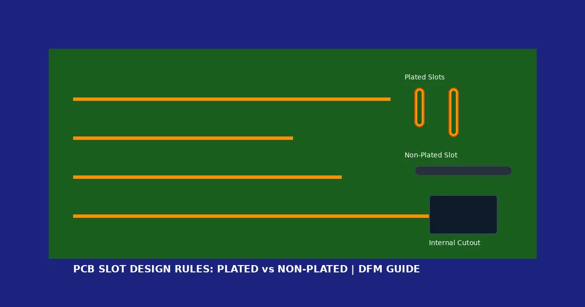
PCB slot design requires understanding two fundamental categories — plated slots (copper-walled, electrically connected, minimum width 0.5 mm) and non-plated slots (bare laminate, minimum width 0.8 mm) — each governed by different manufacturing constraints. Plated slots must observe the same aspect ratio limits as plated through-holes (typically 8:1 for standard processes), require rounded slot ends rather than sharp corners, and must maintain annular ring integrity along the entire slot perimeter. Non-plated slots and internal cutouts require minimum 0.15 mm copper pullback from the routed edge and must be defined on the mechanical or board outline layer — never on the drill file as oversized holes. The most common DFM failure is specifying slots in the wrong CAD layer, causing fabricators to either miss the feature entirely or manufacture it with incorrect plating status.
Why PCB Slot Design Causes More DFM Rejections Than You Expect
Among the thousands of PCB designs that pass through a fabrication facility each month, slot-related engineering queries account for a disproportionate share of DFM holds. The reason is straightforward: most PCB design training focuses on round holes and standard vias, treating slots as a special case that designers encounter infrequently and learn to specify through trial and error. When a design arrives at the CAM department with slots defined ambiguously — a rectangular pad with no corresponding drill feature, a plated slot drawn on the board outline layer, or a cutout specified as an oversized hole in the drill file — production stops while engineers exchange clarification emails. Each query adds three to five days to the delivery schedule.
The underlying manufacturing processes for PCB slots are well-established and highly capable. Modern CNC routing equipment can produce slots with ±0.05 mm positional accuracy and ±0.08 mm dimensional tolerance. The challenge is not fabrication capability but communication clarity: ensuring that your design files unambiguously convey the slot’s location, dimensions, plating requirement, and relationship to surrounding copper features. This guide addresses that challenge systematically, covering the physical manufacturing constraints that drive design rules, the correct methods for defining slots in your CAD environment, and the specific DFM parameters that determine fabrication success.
Understanding PCB Slot Manufacturing Processes
How Plated Slots Are Fabricated
The manufacturing sequence for plated slots follows the same fundamental process as plated through-holes, with adaptations for the elongated geometry. Understanding this sequence explains why certain design rules exist and why they cannot be relaxed without compromising reliability.
For short plated slots (length less than approximately 2.0 mm), most fabricators use the overlapping drill method. The CNC drilling machine places multiple hits along the slot length using a standard drill bit, with each hit overlapping the previous one by approximately 40-60% of the drill diameter. This creates an elongated opening with a scalloped interior surface. The subsequent electroless copper and electrolytic plating processes fill the scallops and produce a reasonably smooth barrel wall. The advantage of this method is speed — it uses existing drilling equipment without switching to a routing spindle — and it ensures the slot is created at the same process stage as other plated holes, guaranteeing correct plating status.
For longer plated slots (length exceeding 2.0 mm), fabricators typically use a routing operation performed before the plating sequence. The CNC router cuts the slot using a small-diameter milling bit that travels along the programmed path. Because this routing occurs before electroless copper deposition and electrolytic plating, the slot barrel receives the same copper treatment as drilled holes. The resulting wall is smoother than the overlapping drill method but requires more precise process control to ensure routing occurs at exactly the right sequence in the manufacturing flow.
The critical point for designers is this: regardless of which method the fabricator chooses, the slot must be defined in the design data in a way that places it into the plated-hole manufacturing stream. Any ambiguity in the design files risks the slot being routed at the wrong process stage — after plating rather than before — resulting in an unplated barrel where plating was required.
How Non-Plated Slots and Cutouts Are Fabricated
Non-plated slots and internal cutouts are manufactured using CNC routing performed after all plating and surface finish processes are complete. This late-stage routing ensures that no copper is deposited on the slot walls. The router bit removes material along the programmed path, leaving bare FR-4 (or other base laminate) exposed at the cut edges.
The routing tool selection depends on the slot geometry. Standard routing uses a 2.0 mm diameter carbide end mill, which produces smooth walls and maintains dimensional accuracy over long production runs. For narrower non-plated slots, tools as small as 0.8 mm diameter can be used, though smaller tools deflect more under cutting forces and wear faster, resulting in slightly wider tolerances.
Internal cutouts — closed shapes completely within the board outline — present a unique challenge because the routing bit must plunge into the laminate to begin cutting. This plunge point creates a small witness mark on one edge of the cutout. For cosmetically sensitive applications, designers should specify the plunge location in the fabrication notes or accept that the fabricator will choose the least visible location.
Complex Slot Features in Your Design?
Upload your Gerber files for a free DFM review. Our CAM engineers will verify slot definitions, check plating status assignments, and confirm all routed features are fabrication-ready before quoting.
Get Free DFM ReviewPlated Slot Design Rules
Minimum Dimensions and Aspect Ratio
Plated slot dimensions are constrained by the same physics that limit plated through-holes: the electroplating process must deposit uniform copper along the entire barrel wall, and the slot must be wide enough for adequate electrolyte circulation during plating.
The minimum plated slot width for most standard-process fabricators is 0.5 mm (20 mil). This limit applies to the finished dimension after plating — the actual routed or drilled opening before plating will be larger by approximately 0.10-0.12 mm to account for copper deposition on both walls. Some manufacturers advertise capabilities down to 0.4 mm, but this typically requires specialized process controls and may involve premium pricing.
The aspect ratio constraint applies to plated slots just as it does to plated through-holes. The aspect ratio is defined as the board thickness divided by the slot width (not length). For standard processes, the maximum aspect ratio is 8:1 to 10:1. This means a 1.6 mm thick board can reliably support plated slots down to 0.2 mm width from an aspect ratio perspective — but the 0.5 mm minimum tool size is the binding constraint in practice. For thick boards (greater than 2.4 mm), the aspect ratio becomes the limiting factor: a 3.2 mm board restricts minimum plated slot width to approximately 0.4 mm at 8:1 or 0.32 mm at 10:1.
Slot length has a practical minimum of twice the slot width, driven by the routing tool geometry. A 0.5 mm wide slot must be at least 1.0 mm long. Shorter slots cannot be produced because the routing bit cannot create an elongated opening shorter than its own diameter without simply producing a round hole.
Annular Ring Requirements for Plated Slots
The annular ring — the copper pad surrounding the slot opening — must maintain minimum width along the entire slot perimeter to ensure reliable solder joints and prevent pad breakout during manufacturing. For plated slots, the annular ring calculation differs from round holes because the pad shape must accommodate the elongated opening.
IPC-6012 Class 2 requires a minimum annular ring of 0.05 mm (2 mil) after all manufacturing tolerances are applied. Class 3 requires 0.05 mm minimum with no breakout permitted. In practice, designers should specify pad dimensions that provide at least 0.15 mm (6 mil) annular ring on each side of the slot to account for registration tolerances and tool wander.
For a 0.6 mm × 2.0 mm plated slot, the minimum pad size should be approximately 0.9 mm × 2.3 mm for Class 2 reliability (providing 0.15 mm annular ring on all sides). The rounded ends of the slot must also maintain annular ring continuity — if your CAD tool generates rectangular pads for oblong holes, verify that the pad corners do not create thin spots where the pad nearly meets the slot edge.
Copper-to-Slot Clearance
Unconnected copper features — traces, planes, and pads belonging to other nets — must maintain clearance from the plated slot edge. This clearance prevents unintended short circuits and provides manufacturing margin for drill registration. The minimum recommended clearance from a plated slot edge to unconnected copper is 0.20 mm (8 mil) for outer layers and 0.25 mm (10 mil) for inner layers, where registration accuracy is slightly lower due to lamination movement.
Ground planes and power planes require thermal relief connections to plated slots, identical to the thermal relief patterns used for plated through-holes. Without thermal relief, the large copper mass makes soldering difficult and increases the risk of cold solder joints during wave soldering or selective soldering operations.
Non-Plated Slot and Internal Cutout Design Rules
Minimum Dimensions for Non-Plated Features
Non-plated slots have a larger minimum width than plated slots because they are cut after plating, using routing tools that must navigate without the structural support of surrounding copper. The standard minimum width for non-plated slots is 0.8 mm (31 mil), corresponding to the smallest routing bit commonly used in production. Some fabricators can achieve 0.6 mm non-plated slots with specialty tooling, but availability and pricing vary.
The minimum length follows the same 2:1 rule as plated slots: a 0.8 mm wide non-plated slot must be at least 1.6 mm long. For wider non-plated cutouts, there is no practical upper limit on dimensions — the routing tool simply traces the programmed path regardless of cutout size.
Internal cutouts (closed shapes within the board) have an additional constraint: the routing tool must have room to maneuver. The minimum internal cutout dimension in any direction is typically 1.0 mm × 1.0 mm for a standard 0.8 mm tool, though a 2.0 mm × 2.0 mm minimum is more practical and produces cleaner results with standard 2.0 mm tooling.
Copper Pullback and Edge Clearance
The most critical design rule for non-plated slots is copper pullback — the minimum distance between any copper feature and the slot edge. This clearance serves several purposes: it prevents copper from being exposed at the cut edge (which could create short circuits or corrosion paths), it provides margin for routing tool positional variation (±0.05 mm typical), and it ensures the routing bit does not contact copper (which would cause accelerated tool wear and produce burrs).
The absolute minimum copper pullback from a non-plated slot edge is 0.15 mm (6 mil). For production reliability, 0.25 mm (10 mil) is strongly recommended. This applies to all copper layers — if an inner layer ground plane extends to within 0.10 mm of a non-plated slot, the exposed copper at the slot edge will be visible as a copper ring or strip, potentially creating reliability concerns in humid environments.
When designing ground plane clearances around non-plated slots, apply the pullback on all copper layers simultaneously. It is a common mistake to clear the outer layers while forgetting that inner layer planes may extend into the clearance zone. Your CAD tool’s keep-out rule should apply the slot clearance constraint to all layers.
Board Edge and Slot Spacing Rules
The minimum distance between a non-plated slot and the board edge (routed outline) is governed by the web strength between the two routed features. If the web is too narrow, it will crack during depanelization or handling. The minimum web width between a slot and the board edge is 1.0 mm for FR-4 at standard 1.6 mm thickness. For thinner boards (0.8 mm or less), increase this minimum to 1.5 mm to prevent breakage.
The same web width rule applies between adjacent slots. Two parallel slots with only 0.5 mm of material between them will produce a fragile web that may crack during thermal cycling, handling, or assembly processes. Maintain at least 1.0 mm between slot edges for structural reliability.
Multiple Slot Types in One Board?
Designs with mixed plated and non-plated slots need careful CAM review. Our engineers verify each slot's process assignment and flag any clearance violations before production begins — preventing costly rework.
Request a QuoteSpecifying Slots Correctly in Your Design Files
The Layer Assignment Problem
The single most common cause of slot-related DFM rejections is incorrect layer assignment. Different CAD tools handle slot definition differently, and the mapping between your CAD’s internal layer names and the final Gerber/Excellon output files is where errors creep in. The fundamental rule is simple but frequently violated: plated slots must appear in the plated drill file, and non-plated slots must appear either in the non-plated drill file or on the mechanical/board outline layer.
In Altium Designer, plated slots are typically defined using the “Slot Hole” primitive on the multi-layer, which exports them to the plated Excellon drill file with a ROUT command. Non-plated slots should be placed on the mechanical layer (Mechanical 1 is standard for board outline and cutouts) or defined on the Keep-Out layer with proper export settings. The critical verification step is opening your exported drill files and confirming that each slot appears in the correct file with the correct plating designation.
In KiCad, the distinction between plated and non-plated slots is controlled by the pad or footprint definition. Plated slots are created as PTH (Plated Through-Hole) pads with oval or custom shapes, while non-plated slots are defined as NPTH pads or drawn on the Edge.Cuts layer for board outline features. KiCad exports these to separate drill files, but designers must verify the export settings match the intended plating assignment.
In Cadence Allegro and OrCAD, slot definition involves the route keepout or mechanical symbol, with manufacturing outputs controlled through the Artwork generation settings. The Gerber and drill file generation process in Allegro provides explicit control over which features appear in which output file, but the complexity of the configuration means errors are common among less experienced users.
Gerber File Best Practices for Slots
Regardless of which CAD tool you use, follow these practices to eliminate slot-related ambiguities in your fabrication data:
Define all non-plated slots and cutouts on a dedicated mechanical layer that is clearly labeled in your output file naming convention. A file named “Board_Outline_And_Cutouts.gbr” or “Mechanical1.gbr” is unambiguous. A file named “Layer14.gbr” invites confusion.
Include a fabrication drawing that explicitly calls out each slot type with dimensions and plating status. Even when your Gerber data is technically complete, a fabrication drawing serves as a human-readable cross-reference that CAM operators use to verify their interpretation of the data. Annotate each slot with “PTH SLOT 0.6 × 2.0 mm” or “NPTH SLOT 1.0 × 3.0 mm” to leave no room for misinterpretation.
Export plated slots using the Excellon drill file format with ROUT commands rather than multiple overlapping drill hits. While both methods produce the same physical result, the ROUT command explicitly communicates the designer’s intent for a continuous slot, whereas overlapping drills could be misinterpreted as a row of individual holes if the overlap is not immediately obvious.
Provide a README or assembly note that lists the total count of each slot type. This gives the fabricator a quick sanity check: “This design contains 4 plated slots (0.6 × 2.0 mm) and 2 non-plated cutouts (5.0 × 10.0 mm).” If their CAM interpretation yields a different count, they know to investigate before proceeding.
Common CAD-to-Fabrication Errors and How to Avoid Them
Several slot definition errors recur across different CAD platforms. Recognizing these patterns helps you catch them during your design review before submitting files for fabrication.
The “oversized hole” error occurs when a designer defines a slot as a single large-diameter circular drill hit in the drill file, expecting the fabricator to interpret it as a slot based on the pad shape visible in the copper layers. This fails because drill files are processed independently of copper data — the fabricator sees only a large round hole, not the oblong pad that motivated the slot. Always define slots as proper routed features, never as oversized round drills.
The “outline layer plated slot” error occurs when plated slots are drawn on the board outline or mechanical layer instead of the drill file. The fabricator routes these features as non-plated cutouts because outline layer features are manufactured in the final routing stage, after all plating is complete. The result is a slot with bare FR-4 walls where copper was required.
The “missing slot” error occurs when a slot exists in the component footprint but is not exported to any output file. This happens when the CAD’s export settings exclude certain pad types or when custom footprints use non-standard layer assignments. Always verify your exported data by opening the Gerber and drill files in a viewer and confirming that every slot in your design appears in the output with correct dimensions and plating status.
Application-Specific Slot Design Guidance
Connector Mounting Slots
Blade-style connectors — USB Type-A, USB Type-C shield tabs, HDMI, D-Sub retention pins, and similar components — are the most common application for plated slots. These components have rectangular or blade-shaped leads that require elongated plated openings for proper insertion and solder joint formation.
When designing pads for connector slots, use the component manufacturer’s recommended footprint dimensions as a starting point, then verify against your fabricator’s capabilities. Many connector datasheets specify the lead cross-section (for example, 0.4 mm × 1.2 mm) but leave the pad and slot dimensions to the designer. A general rule is to add 0.10-0.15 mm to each dimension of the lead cross-section for the finished slot size, providing adequate clearance for component insertion while maintaining enough contact area for reliable solder joints.
For USB Type-C connectors specifically, the through-hole mounting tabs typically require plated slots of approximately 0.6 mm × 1.7 mm with tight positional tolerance (±0.10 mm) to ensure the connector sits flush against the board surface. These connectors also have multiple shell-ground tabs that may use smaller plated slots or standard round plated holes depending on the connector variant.
Voltage Isolation Slots
Non-plated slots are frequently used as creepage and clearance barriers in power supply designs and high-voltage circuits. By removing the PCB substrate between two conductors, the slot forces the leakage path through air (which has significantly higher dielectric strength than FR-4) and increases the effective creepage distance along the board surface.
For safety-agency compliance (IEC 62368-1, IEC 60950-1), the slot width must satisfy both clearance (straight-line air distance across the slot) and creepage (surface distance around the slot ends) requirements for the applicable voltage level and pollution degree. A common approach is to use a slot width of 2.0-3.0 mm for reinforced insulation at mains voltage levels, with the slot length extending far enough that the surface path around the ends also satisfies creepage requirements.
When using isolation slots, ensure that no copper traces, planes, or fills cross the slot on any layer. A ground plane that bridges across the slot on an inner layer completely defeats the isolation purpose. Apply keep-out zones that span the full slot length plus the required creepage distance beyond each slot end, and apply this keep-out to all copper layers in your design.
Thermal Management Slots
Slots can serve as thermal barriers or airflow channels in designs where heat must be directed away from sensitive components. A row of non-plated slots between a high-power section and a temperature-sensitive analog section creates a thermal impedance boundary that reduces conductive heat transfer through the PCB substrate.
The effectiveness of thermal isolation slots depends on the total slot area relative to the remaining thermal path. A single narrow slot provides minimal benefit because heat simply conducts around it through the remaining material. Multiple parallel slots, or a single wide slot spanning the full board width between thermal zones, creates a more effective barrier. In practice, a slot pattern that removes at least 70% of the substrate cross-section between zones provides meaningful thermal isolation.
For airflow slots (commonly used in vertically-mounted boards within forced-air-cooled enclosures), the slot dimensions must balance thermal benefit against structural integrity. Slots larger than 20 mm in length should incorporate small material bridges (tabs) at intervals to prevent board flexure. These tabs can be as narrow as 1.0 mm and placed every 15-20 mm along the slot length.
High-Voltage Isolation or Thermal Slot Design?
Our engineers review slot placements against IPC-2221 creepage tables and verify thermal barrier effectiveness. Upload your design files for expert DFM feedback on isolation and thermal management features.
Upload Design FilesManufacturing Tolerance and Quality Considerations
Dimensional Tolerances for Routed Slots
Understanding manufacturing tolerances helps designers set realistic expectations and avoid over-specifying dimensions that drive up cost. Standard slot tolerances for most PCB fabricators are:
Slot width: ±0.08 mm (±3.1 mil) for standard processes. This tolerance accounts for tool wear, material variation, and CNC positioning accuracy. For tighter requirements (±0.05 mm), specify this explicitly in your fabrication notes — many fabricators can achieve it with tool compensation adjustments, but it requires awareness during CAM setup.
Slot length: ±0.10 mm (±4 mil) for standard processes. Length tolerance is slightly larger than width because it accumulates over the routing path distance.
Slot position: ±0.05 mm (±2 mil) relative to drilled hole patterns, and ±0.10 mm (±4 mil) relative to copper features. Positional accuracy is determined by the CNC equipment’s registration to the panel fiducials and is typically the tightest specification in the slot tolerance stack.
For plated slots, the finished dimension after plating will be smaller than the routed opening by approximately 0.050-0.060 mm (total, both walls) due to copper deposition. Fabricators account for this when selecting their routing program dimensions, but the finished tolerance on the delivered board remains ±0.08 mm from the nominal specified by the designer.
Quality Verification and Inspection Methods
Fabricators use several methods to verify slot quality during production:
Optical inspection verifies slot dimensions, position, and surface condition on outer layers. Automated optical inspection (AOI) systems can measure slot width and length and compare against programmed targets, flagging any slots that exceed tolerance limits.
Cross-section analysis is used for plated slots to verify copper thickness uniformity along the barrel walls. Because plating distribution in elongated openings differs from round holes (corners and endpoints tend to receive more plating than the center of long walls), cross-sectioning confirms that minimum thickness requirements are met at the weakest point.
Electrical testing (flying probe or fixture) verifies that plated slots provide electrical continuity between layers and that non-plated slots maintain isolation. This is particularly important for voltage isolation slots, where even a thin copper bridge across the slot would defeat its purpose.
Design Rule Summary Table
The following parameters represent conservative, production-proven values suitable for standard FR-4 multilayer PCBs at 1.6 mm thickness. For non-standard board thicknesses, materials, or layer counts, consult your fabricator’s capability documentation or request a manufacturability review.
Plated slot minimum width: 0.5 mm finished. Plated slot minimum length: 1.0 mm (or 2x width, whichever is greater). Plated slot aspect ratio limit: 8:1 (board thickness divided by slot width). Plated slot annular ring minimum: 0.15 mm per side (Class 2), 0.15 mm with no breakout (Class 3). Plated slot copper clearance to non-net copper: 0.20 mm outer layers, 0.25 mm inner layers.
Non-plated slot minimum width: 0.8 mm. Non-plated slot minimum length: 1.6 mm (or 2x width). Non-plated slot copper pullback: 0.25 mm recommended (0.15 mm absolute minimum). Minimum web between slots: 1.0 mm. Minimum web between slot and board edge: 1.0 mm. Internal cutout minimum dimension: 2.0 mm × 2.0 mm (with standard 2.0 mm tool).
Tolerances: Width ±0.08 mm, Length ±0.10 mm, Position ±0.05 mm to drill patterns, ±0.10 mm to copper features.
Avoiding the Most Common Slot DFM Failures
Over years of processing customer designs, certain slot-related errors appear repeatedly. Understanding these failure modes helps designers implement checking procedures that catch problems before fabrication submission.
The number one failure is plating status ambiguity — the fabricator cannot determine whether a slot should be plated or non-plated from the design data alone. This happens when slots appear only in the copper layers (as oblong pads) without corresponding entries in either the plated drill file or the mechanical outline file. Prevention: always verify that every slot in your design appears in exactly one output file — either the plated drill file or the non-plated features file — and never in both.
The second most common failure is insufficient copper pullback on inner layers. Designers clear the outer layer copper around non-plated slots but forget that inner layer planes extend to the slot edge. When the router cuts through these planes, it exposes bare copper at the slot edge, creating potential corrosion and reliability issues. Prevention: apply slot clearance rules to all copper layers in your design rule settings.
The third failure is specifying slots that violate the aspect ratio for the board thickness. A 0.5 mm wide plated slot on a 3.2 mm thick board has an aspect ratio of 6.4:1, which is within capability. But a 0.4 mm wide slot on the same board pushes to 8:1, and a 0.3 mm slot at 10.7:1 exceeds most standard processes. Prevention: calculate the aspect ratio for every plated slot in thick board designs and verify against your fabricator’s published capability.
Eliminate Slot-Related DFM Rejections
Our free DFM review catches plating status ambiguities, clearance violations, and aspect ratio concerns before your board enters production. Most issues are resolved within 24 hours.
Submit Files for DFM ReviewReviewed by AtlasPCB Engineering Team
This guide reflects fabrication parameters validated across our standard and advanced manufacturing processes. Slot capabilities may vary for non-standard substrates (ceramic, metal-core, flex), extreme layer counts (20+), or specialty surface finishes. Contact our engineering team for design-specific consultation on complex slot requirements.
About AtlasPCB — We specialize in complex PCB manufacturing for HDI, RF, and high-reliability applications. Explore our free engineering DFM review . Every order includes free engineering review. Get your quote.
Reviewed by AtlasPCB Engineering Team — IPC-certified manufacturing specialists with 15+ years of production experience in HDI, RF, and high-reliability PCB fabrication. Content based on factory floor data and real customer design reviews.
Frequently Asked Questions
What is the minimum width for a plated PCB slot?
How do I specify a non-plated slot in my Gerber files?
What clearance is needed between a non-plated slot and copper features?
Can I have sharp corners in a PCB slot?
- PCB slots
- routed features
- DFM
- plated slots
- non-plated slots
- PCB cutouts
- fabrication drawing
- Gerber files