· AtlasPCB Engineering Team · Engineering · 20 min read
PCB Prepreg vs Core: A Manufacturer's Guide to Stackup Materials, Pressed Thickness, and Specification Mistakes
Understand the real differences between PCB prepreg and core from a manufacturer's perspective. Includes pressed thickness data, resin starvation failures, glass weave selection, and the specification mistakes that add cost to your order.
Quick Answer
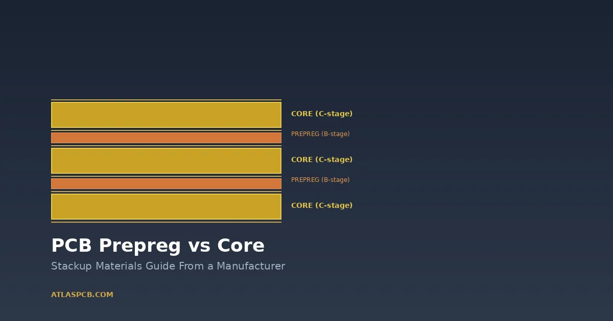
PCB core is a fully cured copper-clad laminate that provides stable dielectric layers for inner-layer circuitry, while prepreg is a partially cured (B-stage) bonding material that flows during lamination to join cores, fill copper relief, and form its final thickness under heat and pressure. The critical distinction for designers is that core thickness is relatively fixed before lamination, whereas prepreg pressed thickness varies depending on adjacent copper coverage, resin content, and press conditions — making accurate impedance modeling dependent on understanding both materials and how your fabricator processes them.
Reviewed by AtlasPCB Engineering Team
Why Engineers Need to Understand Both Materials
Every multilayer PCB is built from two fundamental dielectric materials: core and prepreg. The distinction between them is not merely academic. When you submit a stackup to a fabricator, the choice of core thickness, prepreg style, and ply count directly determines your dielectric spacing, impedance values, and whether the board will survive thermal cycling without delamination. Getting this wrong is one of the most common sources of engineering queries that delay orders and add cost.
In our lamination department at AtlasPCB, we process dozens of different stackup configurations daily. The most frequent problems we encounter are not exotic material failures. They are straightforward specification errors — designers who confuse core thickness with dielectric thickness, specify unavailable prepreg styles copied from a different fabricator’s stackup, or underestimate the resin volume needed for their copper distribution. These mistakes are preventable once you understand what core and prepreg actually are, how they behave during manufacturing, and what your fabricator needs from your specification.
This guide covers both materials from a manufacturer’s perspective, with real production data on pressed thickness, glass weave selection, and the specification practices that keep your order on schedule and your impedance on target.
What Core and Prepreg Actually Are
The terms core and prepreg describe two different physical states of what is essentially the same base material system: woven glass fiber reinforced with epoxy resin.
A PCB core is a fully cured laminate. The resin has completed its cross-linking reaction, the material has reached its final mechanical and electrical properties, and copper foil has been bonded to both sides during the original laminate manufacturing process. When you receive a core from a material supplier, it is rigid, dimensionally stable, and ready for inner-layer imaging and etching. The copper-clad core is the starting point for creating your inner-layer circuit patterns. After imaging and etching, the core carries a finished copper pair — one circuit layer on each face — separated by a dielectric layer with known, stable properties.
Prepreg, by contrast, is the bonding agent that holds a multilayer PCB together. It consists of the same glass fiber weave impregnated with the same resin system, but the resin has only been partially cured to what material scientists call the B-stage. In this state, the resin is solid at room temperature but will soften and flow when heated. During the lamination press cycle, the prepreg is placed between etched cores (or between a core and an outer copper foil), and the entire stack is subjected to temperatures typically between 170 and 185 degrees Celsius under pressures of 250 to 400 psi. The resin softens, flows into the etched copper relief on adjacent layers, wets and bonds to all surfaces, and then completes its cross-linking cure to become a fully hardened dielectric.
This distinction — cured versus partially cured — is what defines every practical difference between the two materials. Core gives you dimensional predictability because its thickness is already set. Prepreg gives you bonding capability because its resin still flows, but that flow means its final thickness depends on what it encounters during pressing.
Glass Weave Styles and Resin Content
Both core and prepreg are built on standardized glass fiber weaves identified by style numbers defined in IPC-4412. The glass weave style determines the physical thickness of the reinforcement fabric, the openness of the weave pattern, and consequently the amount of resin that can be carried within and around the glass fibers. Understanding these styles matters because they directly control dielectric thickness, resin availability for copper fill, and the dielectric constant of the finished layer.
The most commonly used glass weave styles in PCB manufacturing are 106, 1080, 2116, 3313, and 7628. Style 106 uses the finest yarn and most open weave, producing the thinnest plies with the highest resin content — typically 70 to 75 percent resin by weight. At the other end of the spectrum, style 7628 uses thick yarn bundles in a tight weave, producing the thickest plies with the lowest resin content at roughly 42 to 48 percent by weight. Style 1080 is the workhorse of the industry for thin dielectric layers, offering a good balance between thickness (nominally 2.6 to 3.0 mils per ply), resin content (around 63 to 68 percent), and mechanical handling during layup.
The resin content percentage is not just a material science detail. It determines how much resin is available to flow and fill the copper relief during lamination. A prepreg with higher resin content can accommodate more copper thickness variation and uneven copper distribution without running into fill problems. This is why fabricators often recommend high-resin prepreg variants (sometimes designated with an “HR” suffix) when your design has heavy copper or large ground plane areas adjacent to sparse routing layers.
In practice, most fabricators maintain inventory of a limited set of glass styles — commonly 1080, 2116, and 7628 for standard FR-4, with 106 and 1067 stocked for specialty applications. When a designer specifies a glass style that the fabricator does not stock, it triggers either a material order (adding days to lead time) or an engineering query proposing an equivalent construction. Our recommendation is to specify your target dielectric thickness and impedance requirements and let the fabricator select the glass style combination that achieves those targets from their qualified inventory. This approach consistently yields faster turnaround and fewer surprises.
How Core and Prepreg Work Together in Multilayer Stackups
A multilayer PCB stackup is assembled by alternating cores and prepreg sheets in a specific sequence that is then bonded together in a lamination press. The exact arrangement depends on the board’s layer count and the construction method chosen by the fabricator, but the fundamental principle is consistent: cores carry copper circuit pairs, and prepreg bonds everything together.
Consider a standard four-layer board built with the most common foil construction. The starting point is a single core — typically 0.028 to 0.040 inches thick for a standard 1.6 mm finished board — with copper on both sides. The inner layers (layers 2 and 3) are imaged and etched on this core. Then one or two sheets of prepreg are placed on each side of the etched core, followed by outer copper foils. The entire sandwich goes into the lamination press, where the prepreg bonds the outer foils to the core, forming the complete four-layer structure. The outer copper foils become layers 1 and 4 after subsequent drilling, plating, and outer-layer imaging.
For a six-layer board, the construction typically uses two cores. Each core carries one inner-layer circuit pair. Prepreg sheets are placed between the two cores and on the outside faces, with outer copper foils completing the stack. The lamination bonds everything into a single rigid structure. For a detailed walkthrough of six-layer stackup configurations, our 6-layer PCB stackup design guide covers the topic extensively.
Eight-layer and higher boards follow the same pattern with additional cores and prepreg layers. However, the construction sequence becomes more complex when blind or buried vias are involved, as these require sequential lamination — building the board in stages with separate press cycles. In a sequential build, some cores are drilled and plated before being laminated with additional prepreg and cores, requiring careful planning of the via structure and lamination sequence.
There are also alternative construction methods worth understanding. In a cap construction, the outermost copper layers are supplied on thin cores rather than bare copper foils, which can improve layer-to-layer registration on the outer layers. In a foil-only construction used for some simple four-layer boards, all dielectric layers are prepreg with no separate core — the entire board is built up from alternating prepreg and copper foil, pressed in a single cycle. Each construction type assigns different roles to core and prepreg, and your fabricator will choose the method that best matches your design requirements and their process capabilities.
Need Help With Your Stackup Design?
Our engineering team reviews every stackup before production, recommending material selections and construction methods optimized for your impedance, thickness, and reliability targets.
Why the Same Material Has Different Dk Values as Core vs Prepreg
One of the most confusing aspects of PCB materials for designers is that core and prepreg from the same product family — same brand name, same resin system — can have different dielectric constant (Dk) values. This is not a manufacturing defect or datasheet error. It is a direct consequence of the structural differences between the two material forms.
The dielectric constant of a glass-reinforced laminate is a composite property determined by the ratio of glass to resin in the signal’s electromagnetic field. Glass has a Dk of approximately 6.1 to 6.7 (depending on glass type), while typical FR-4 epoxy resin has a Dk of roughly 3.0 to 3.5. The effective Dk of the laminate is a weighted average of these two constituents based on their volume fractions in the region where the signal propagates.
Core materials have a fixed glass-to-resin ratio established during their original manufacture. Prepreg of the same glass style starts with a different resin content (usually higher to provide fill capacity) and then changes during lamination as resin flows out of the prepreg sheet and into adjacent copper relief. After pressing, the cured prepreg layer may have a different effective glass-to-resin ratio than the corresponding core material, even though they started from the same base components.
For standard FR-4 materials like Shengyi S1000-2M or Isola IS370HR, the Dk difference between core and prepreg of the same glass style is typically 0.1 to 0.3 units at 1 GHz. That may sound small, but for controlled impedance designs targeting 50 ohms on thin dielectric layers, a Dk shift of 0.2 can change the calculated trace width by 0.5 to 1.0 mils — enough to push an impedance result outside specification.
This is why your impedance calculation must use the correct Dk value for each dielectric layer based on whether it is formed from core or prepreg, and ideally from the specific glass style and resin content in that layer. Most fabricators provide their own impedance models calibrated to their actual press conditions and material lots, which is more reliable than using generic datasheet values. When we run impedance modeling at AtlasPCB, we use our press-validated Dk values that account for resin flow, which typically differ from the supplier’s nominal datasheet figures by 2 to 5 percent.
Pressed Thickness: The Number Your Impedance Model Actually Needs
This is where the practical reality of prepreg diverges most significantly from what many designers assume. The thickness listed on a prepreg datasheet — the nominal thickness — is measured on a single uncured sheet before lamination. It is not the thickness of the dielectric layer in your finished board.
During lamination, prepreg resin flows to fill the etched copper relief on adjacent layers, and the glass weave compresses slightly under press pressure. The result is that pressed prepreg thickness is always less than nominal thickness, and the amount of reduction depends directly on the copper coverage of the adjacent layers.
Here is an example using real production data from our facility for a standard 1080 glass style prepreg (Shengyi S1000-2M, standard resin content). The nominal thickness per ply is approximately 2.8 mils (0.071 mm):
Adjacent copper coverage at 75 percent or higher, as you would see between large ground or power planes, produces a pressed thickness of approximately 2.0 to 2.3 mils per ply. Adjacent copper coverage around 50 percent, typical of moderate-density routing layers, presses to approximately 2.3 to 2.5 mils. Adjacent copper coverage at 25 percent or lower, as seen with sparse routing, gives a pressed thickness of approximately 2.5 to 2.8 mils.
The variation is not trivial. Between a ground plane pair (high copper coverage) and a sparse signal layer (low coverage), the same single ply of prepreg can produce a dielectric thickness difference of 0.5 to 0.8 mils. For a 50-ohm microstrip on a 3-mil dielectric, that represents a potential impedance shift of 5 to 8 ohms if the wrong thickness assumption is used in the calculation.
This is precisely why fabricators insist on providing impedance-modeled stackups rather than accepting designer-specified dielectric thicknesses at face value. When we model a stackup at AtlasPCB, we calculate pressed thickness for each prepreg layer based on the actual copper distribution on adjacent layers — information we extract from the Gerber files. If you specify a target dielectric thickness that cannot be achieved with our available prepreg combinations and your specific copper pattern, we will propose an adjusted stackup and issue a query explaining the change.
For board thickness tolerance specifications, the accumulated pressed thickness variation across all prepreg layers is one of the primary contributors to total stackup thickness tolerance. Designs with many prepreg layers naturally have wider thickness tolerances than designs built primarily on cores.
Resin Starvation and Fill Failures
Resin starvation is one of the most serious lamination defects in multilayer PCB manufacturing, and it occurs when there is not enough resin in the prepreg to completely fill the copper relief on adjacent layers. The consequences range from cosmetic voids visible in cross-section to catastrophic delamination failures during thermal cycling or soldering.
When a fabricator etches inner-layer copper patterns, the etched-away areas create channels and voids in the copper surface. During lamination, prepreg resin must flow into these channels to create a solid, void-free bond between layers. The total volume of resin needed depends on the copper thickness, the percentage of copper removed by etching, and the uniformity of the copper distribution across the panel.
The risk increases dramatically with heavy copper designs. A standard 1-ounce (35 micrometer) copper layer with 50 percent copper removal creates etch channels roughly 1.4 mils deep. A 2-ounce (70 micrometer) layer with the same pattern creates channels 2.8 mils deep — requiring roughly twice the resin volume to fill. For heavy copper PCB designs, this resin demand can exceed what a single prepreg ply provides, requiring multiple plies or higher-resin-content prepreg selections.
The situation becomes more challenging when copper distribution is uneven. Consider a layer that has a large ground plane covering 90 percent of one region of the board and sparse traces covering only 15 percent of another region. The prepreg resin will flow preferentially toward the areas with the most copper relief (the sparse trace region), potentially leaving the plane region with insufficient bonding. This differential flow can create localized resin starvation even when the average resin volume seems adequate.
In our production experience, we see resin starvation issues most commonly in three scenarios: designs with 2-ounce or heavier copper and insufficient prepreg plies, designs with extreme copper density imbalance between adjacent layers, and designs where the stackup was copied from a different fabricator without verifying resin sufficiency for the new press conditions. Prevention is straightforward — use the copper balancing and thieving techniques to equalize copper distribution, specify adequate prepreg plies for your copper weight, and let your fabricator validate resin sufficiency as part of their DFM review.
Five Specification Mistakes That Add Cost or Delay Your Order
After processing thousands of unique PCB designs, we have identified a consistent set of specification errors in stackup callouts that trigger engineering queries, delay production starts, and sometimes add unnecessary cost. Each of these is easily avoidable once you understand what the fabricator needs.
The first mistake is confusing core thickness with dielectric thickness. Core thickness, as listed on supplier datasheets, includes the base laminate plus any copper cladding that was part of the original manufacture. The dielectric thickness — the actual insulating distance between copper layers — is the core thickness minus the copper on each side. When a designer specifies a core dielectric of 8 mils but the supplier’s 8-mil core actually has a 7.1-mil dielectric after accounting for the base copper weights, the impedance calculation will be off. Always confirm whether the thickness in your stackup notes refers to overall core thickness or dielectric-only.
The second mistake is specifying exact prepreg style numbers copied from another fabricator’s stackup. If your previous fabricator used “2 plies of 2116” for a particular dielectric layer, it does not mean the next fabricator stocks 2116 or runs the same press profile. Specifying a target dielectric thickness with an acceptable tolerance range gives the new fabricator flexibility to use their qualified equivalent, which often means faster turnaround and lower cost.
The third mistake is over-constraining the material brand. Unless your application genuinely requires a specific material family for electrical or regulatory reasons (such as Rogers RO4350B for an RF design or a specific UL-listed material for safety certification), specifying “Isola 370HR only” when a Shengyi S1000-2M with equivalent properties is available at lower cost and shorter lead time will penalize your budget. Specify the performance requirements — Dk, Df, Tg, CTI, flammability rating — and let the fabricator propose qualified materials that meet them.
The fourth mistake is neglecting to specify impedance targets on the fabrication drawing when the design requires impedance control. Some designers embed impedance assumptions into their stackup notes without explicitly calling out controlled impedance as a requirement. If your fabrication drawing does not include impedance callouts, the fabricator may build the board without impedance verification, and you will only discover the problem during your own testing. Our DFM checklist for PCB designers covers the essential callouts that should appear on every fabrication drawing.
The fifth mistake is specifying asymmetric stackups without understanding the consequences. A stackup where the prepreg and core arrangement is not symmetric about the board’s center line will cause warpage during lamination and thermal cycling. While some designs legitimately require asymmetric constructions, many cases we see are unintentional — the designer assigned layer thicknesses without checking symmetry. The fabricator will flag this and propose a symmetric alternative, but the discussion adds time to your order.
Avoid DFM Delays on Your Next Order
Upload your design files and our engineering team will review your stackup, material selections, and impedance requirements before production starts — catching specification errors before they become costly delays.
How Material Selection Affects PCB Cost and Lead Time
The choice of core and prepreg materials affects your PCB pricing through three mechanisms: material cost itself, inventory availability, and process complexity.
Standard FR-4 materials (Tg 130 to 140 degrees Celsius) from major Chinese suppliers like Shengyi and KB are the least expensive and most widely stocked. Moving to mid-Tg FR-4 (Tg 150 to 170) adds a modest premium of roughly 5 to 10 percent, primarily because these materials use modified resin systems with higher cross-link density. High-Tg and halogen-free materials (Tg 170 and above) can add 10 to 25 percent depending on the specific product, and low-loss high-speed materials like Shengyi S1000-2M or Isola IS370HR add 15 to 30 percent over standard FR-4.
The cost impact becomes more significant with specialty materials. Rogers high-frequency laminates can cost 3 to 8 times more than standard FR-4 depending on the specific product, and they typically require special ordering with lead times of 2 to 4 weeks for the raw material alone. Hybrid stackups that combine Rogers cores with FR-4 or compatible low-loss prepreg can reduce this cost premium significantly while maintaining high-frequency performance on critical layers, as discussed in our Rogers PCB material guide.
The number of prepreg plies in a stackup also affects cost, though less dramatically than the material grade. Each additional prepreg ply adds material cost and slightly extends layup time. However, trying to minimize cost by using fewer prepreg plies than the design requires is false economy — if insufficient resin leads to a lamination failure, the entire panel must be scrapped and rebuilt, which costs far more than the extra sheet of prepreg.
Fabricators stock specific core thicknesses and prepreg styles based on their most common orders. At AtlasPCB, our standard FR-4 inventory covers core thicknesses from 0.1 mm to 1.6 mm in common increments, and prepreg styles 1080, 2116, and 7628 in standard and high-resin variants. Designs that require non-standard core thicknesses or unusual prepreg configurations may need special material orders, adding 3 to 7 business days to production lead time. For quick-turn PCB orders, using standard materials from our inventory eliminates this delay.
How to Specify Core and Prepreg on Your Fabrication Drawing
The fabrication drawing is your contract with the manufacturer. Getting the material specification right means communicating your requirements clearly while leaving appropriate flexibility for the fabricator to optimize production.
For standard FR-4 multilayer boards, the most effective specification approach includes the following elements. First, specify the material performance class rather than a brand name: “FR-4, Tg 150 minimum, IPC-4101/126 or equivalent.” Second, provide your target stackup with layer-by-layer dielectric thickness targets and acceptable tolerances: “Dielectric L2-L3: 8 mil nominal, plus or minus 1.5 mil.” Third, call out impedance requirements explicitly: “50 ohm single-ended, 100 ohm differential, plus or minus 10%, layers 1 and 6 referenced to adjacent planes.” Fourth, note any special material requirements that are genuinely necessary: “Lead-free compatible, halogen-free per IPC-4101B, Appendix A required.”
What to avoid: do not copy a specific stackup table from another fabricator’s documentation and include it as a mandatory specification. That stackup was designed around their inventory, press conditions, and impedance correlation data. Instead, provide your dielectric targets and impedance requirements and request the fabricator’s proposed stackup for review.
For more complex materials — mixed dielectric stackups, Rogers or PTFE layers, or controlled-Dk requirements above standard FR-4 — more detailed material callouts are appropriate. In these cases, specifying the material family (such as “Rogers RO4350B core for layers 3-4”) is justified because the electrical properties are not interchangeable with other materials.
A well-written fabrication specification for our Gerber file submission process communicates your design intent without constraining the fabricator unnecessarily. The goal is a board that meets your electrical, mechanical, and reliability requirements at the lowest cost and fastest turnaround, and that requires a collaborative approach to material selection between designer and manufacturer.
Ready to Order?
Upload your Gerber files and stackup requirements. Our engineers will propose an optimized material combination, verify impedance, and confirm lead time before production begins.
Making the Right Material Choices
The distinction between core and prepreg is fundamental to multilayer PCB design, but the practical implications extend far beyond knowing which one is cured and which one flows. Your material selections affect impedance accuracy, lamination reliability, manufacturing cost, and production lead time. Understanding how these materials behave in real manufacturing — pressed thickness variation, resin flow dynamics, and the practical limits of glass style availability — transforms stackup design from an abstract exercise into a manufacturing-aware decision process.
The most successful approach we see from experienced designers is one of informed collaboration. Specify your performance requirements precisely — impedance targets, dielectric thickness goals, material performance class, and reliability requirements. Then work with your fabricator to translate those requirements into a production-ready stackup built from qualified, available materials processed under validated conditions. This partnership consistently produces better results than either over-specifying every material detail or leaving everything unspecified and hoping for the best.
Every stackup we build at AtlasPCB goes through this collaborative review process, and the boards that emerge from it meet their targets with fewer engineering queries, faster production starts, and better first-pass yields than designs where the material specification was treated as an afterthought.
About AtlasPCB — We specialize in complex PCB manufacturing for HDI, RF, and high-reliability applications. Explore our impedance-controlled PCB manufacturing, or get an free engineering DFM review . Every order includes free engineering review. Get your quote.
Reviewed by AtlasPCB Engineering Team — IPC-certified manufacturing specialists with 15+ years of production experience in HDI, RF, and high-reliability PCB fabrication. Content based on factory floor data and real customer design reviews.
Frequently Asked Questions
What is the difference between prepreg and core in a PCB?
Does prepreg thickness change during PCB lamination?
How do I choose between different prepreg glass weave styles?
Can I mix different material brands for core and prepreg in the same PCB?
What causes resin starvation in PCB lamination?
- pcb prepreg
- pcb core
- multilayer stackup
- pcb lamination
- pcb materials
- impedance control
- dfm