· Atlas PCB Engineering Team · Engineering · 14 min read
PCB Etch Factor and Trace Width Compensation: A DFM Guide for Precision Etching
Understanding etch factor and trace width compensation is essential for achieving target trace widths in PCB manufacturing. This guide explains how copper etching undercut affects conductor geometry, how fabricators calculate compensation values, and what designers should specify to ensure impedance-controlled traces meet their targets.
Why Etch Factor Matters in PCB Manufacturing
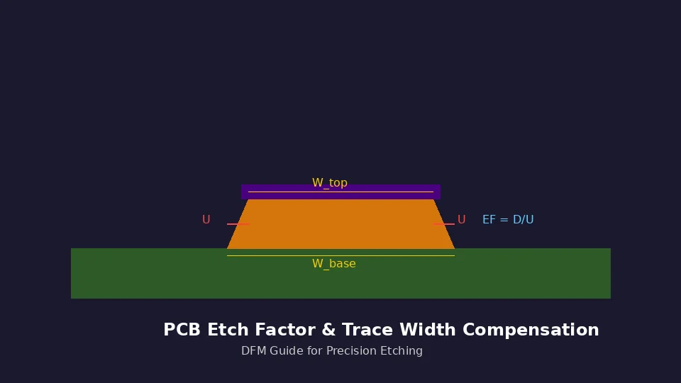
Every copper trace on a printed circuit board begins life wider than it ends up. During the subtractive etching process — still the dominant method for forming conductors on standard PCB constructions — chemical etchant dissolves copper not only downward through the exposed areas but also laterally beneath the etch resist. This lateral dissolution, known as undercut, produces traces with a characteristic trapezoidal cross-section rather than the ideal rectangular profile that design software assumes.
The ratio between the depth of etch (copper thickness) and the lateral undercut distance is called the etch factor. For PCB designers targeting controlled impedance lines or minimum spacing requirements, understanding etch factor is not optional — it directly determines whether the finished board meets electrical specifications. A designer who ignores etch compensation may find that a 4-mil target trace measures only 3.2 mils at the base after etching, fundamentally changing the line’s characteristic impedance.
At AtlasPCB, our engineering team reviews every impedance-controlled design for appropriate etch compensation before fabrication begins. This article explains the physics behind etch factor, how compensation values are calculated, and what designers should specify in their fabrication notes to achieve first-pass success.
The Physics of Chemical Etching
Subtractive PCB etching uses chemical solutions — most commonly cupric chloride (CuCl2) or ammoniacal etchant — to dissolve unwanted copper from a panel. The process begins after photoresist has been imaged and developed, leaving resist patterns that protect the intended conductor areas.
When etchant contacts exposed copper, it dissolves the metal isotropically — meaning it attacks from all directions simultaneously. While the etchant primarily works downward through the exposed copper thickness, it also works laterally underneath the resist edges. The result is that the finished conductor is narrower than the resist pattern that defined it, with the narrowing occurring on both sides of the trace.
The degree of undercut depends on several interacting factors. Copper thickness is the most significant variable because thicker copper requires longer etch times, giving the etchant more opportunity to work laterally. A 2-oz (70-micron) copper layer experiences substantially more undercut than a half-ounce (17.5-micron) layer simply because the panel spends roughly four times longer in the etch chamber.
Etchant chemistry also plays a role. Cupric chloride systems, which dominate in horizontal conveyorized etching lines, provide relatively consistent etch rates and moderate etch factors in the range of 2.5 to 3.5 for standard process conditions. Ammoniacal etchants can achieve higher etch factors (3.0 to 4.0) but are more sensitive to process parameter variations. The trade-off between etch factor performance and process stability influences which chemistry a fabricator selects for different product types.
Equipment configuration matters as well. Modern horizontal spray-etching machines use oscillating nozzles, controlled spray pressures, and precise conveyor speeds to optimize etch uniformity. The spray pressure and angle affect how quickly fresh etchant reaches the copper surface and how efficiently spent etchant is removed from the reaction zone. Higher spray pressures generally improve the etch factor by directing etchant more vertically, but excessive pressure can damage fine-line resist patterns.
Defining Etch Factor Mathematically
The etch factor (EF) is formally defined as the ratio of the etch depth to the lateral undercut on one side:
EF = D / U
Where D is the total depth of etch (equal to the copper thickness) and U is the lateral undercut distance measured from the resist edge to the point where the copper sidewall meets the base. A higher etch factor indicates less lateral undercut relative to the copper thickness, which is always desirable.
For a trace with resist width W_resist, the finished trace width at the copper base (W_base) is:
W_base = W_resist - 2U = W_resist - 2(D/EF)
And the finished trace width at the top (W_top) equals the resist width minus a small amount of top-corner rounding:
W_top is approximately equal to W_resist
This creates the characteristic trapezoidal profile where the top of the trace is wider than the base. For impedance calculations, the effective electrical width is typically taken as the average of top and base widths:
W_effective = (W_top + W_base) / 2
Understanding this geometry is critical because impedance modeling tools like Polar Si9000 or Ansys 2D Extractor can model trapezoidal conductors explicitly. When a designer specifies a target trace width, the fabricator must determine what resist width (artwork compensation) will produce that target after etching.
Typical Etch Factor Values by Copper Weight
Etch factor varies with copper thickness and process capability. The following values represent achievable performance on modern horizontal spray-etching equipment under controlled production conditions:
For half-ounce copper (17.5 micrometers), etch factors typically range from 3.0 to 4.0. The thin copper layer requires minimal etch time, limiting lateral undercut to approximately 4.4 to 5.8 micrometers per side. This makes half-ounce copper the preferred starting point for fine-line designs below 4-mil trace widths.
One-ounce copper (35 micrometers) produces etch factors between 2.5 and 3.5 in most production environments. The undercut per side ranges from 10 to 14 micrometers (0.4 to 0.55 mils). This is the most common copper weight for impedance-controlled designs and represents the sweet spot between current-carrying capacity and trace definition quality.
Two-ounce copper (70 micrometers) challenges even the best etching processes, with etch factors dropping to 2.0 to 3.0. Undercut per side reaches 23 to 35 micrometers (0.9 to 1.4 mils), meaning each trace narrows by 1.8 to 2.8 mils total. Designers using 2-oz copper for power planes or high-current traces must account for substantial width reduction when defining clearances and spacing.
Three-ounce copper and heavier constructions push etch factors below 2.5 in most cases, making subtractive etching increasingly impractical for fine features. Many fabricators transition to pattern plating or additive processes for heavy copper applications requiring trace widths below 8 mils.
How Fabricators Apply Compensation
When a PCB fabricator receives design data for an impedance-controlled board, the engineering team performs etch compensation as part of CAM processing. The compensation process works backward from the target finished trace width to determine the required artwork (resist) width.
The basic compensation formula is:
W_resist = W_target + 2(D/EF) - correction_factors
In practice, the fabricator’s process engineers maintain empirical compensation tables based on production data rather than relying solely on theoretical calculations. These tables account for the specific etchant chemistry, equipment configuration, copper foil type (standard electrodeposited versus rolled annealed), and even the board’s position within the panel.
The compensation is applied in the CAM system by bloating trace features outward symmetrically. A 5-mil target trace on 1-oz copper with an expected etch factor of 3.0 would receive approximately 0.47 mils of compensation per side (35/3.0 = 11.7 micrometers = 0.46 mils), resulting in an artwork width of approximately 5.9 mils. The exact value depends on the fabricator’s specific process capability data.
Importantly, compensation values are not uniform across a panel. Traces in the center of a large copper area may etch slightly differently than isolated traces, and outer-layer traces behave differently from inner-layer traces because outer layers use conveyorized spray etching while inner layers may use different equipment configurations. Sophisticated CAM systems can apply location-dependent compensation rules.
Impact on Impedance Control
For impedance-controlled designs, etch factor directly affects whether the finished trace width produces the target characteristic impedance. A 1-mil deviation in trace width typically shifts impedance by 3 to 8 ohms depending on the stackup geometry, making precise etch compensation essential for meeting standard tolerances of plus or minus 10 percent.
Consider a 50-ohm single-ended microstrip on a 4-mil dielectric with 1-oz copper. The target trace width might be 7.2 mils based on impedance modeling. If the fabricator’s etch factor is 3.0, the required compensation is approximately 0.9 mils total (0.45 mils per side), giving an artwork width of 8.1 mils. If the actual etch factor on that production run comes in at 2.5 instead of 3.0, the trace will be approximately 0.5 mils narrower than target, pushing impedance up by 2 to 4 ohms.
This is why fabricators maintain statistical process control (SPC) data on their etch factor performance. Consistent etch factor enables tighter impedance control because the compensation values remain predictable from lot to lot. AtlasPCB monitors etch factor trends on every production panel using cross-section analysis and automated optical measurement, feeding data back into compensation tables in near-real-time.
Differential pairs add another dimension of complexity. Both the trace width and the gap between paired traces are affected by etching. If a differential pair has a designed gap of 5 mils between traces, the actual post-etch gap will be wider than drawn because both adjacent trace edges undercut inward. The gap increases by twice the single-side undercut value. This gap widening reduces the coupling between differential traces, affecting differential impedance.
Design Guidelines for Etch-Friendly Layouts
Designers can significantly improve manufacturing yield by following etch-aware design practices. The first principle is matching copper weight to feature requirements. Using 1-oz copper when half-ounce would meet current-carrying needs wastes etch factor margin and limits achievable trace/space resolution.
Minimum trace width should be specified relative to copper thickness. A practical rule of thumb is that the minimum reliable trace width equals three times the copper thickness for standard etch processes. For 1-oz copper (35 micrometers), this suggests a 4.1-mil minimum — which aligns with most fabricators’ standard capability limits. Going below this ratio requires advanced process controls and acceptance of higher scrap rates.
Uniform copper distribution across a layer improves etch consistency. Large open areas adjacent to fine traces create etch loading effects where the etchant concentration varies locally. Adding copper fill (ground pour) to open areas equalizes the copper density and produces more uniform etch results across the panel.
For impedance-critical nets, avoid routing traces adjacent to board edges or panel rails where etch uniformity is typically poorest. The first and last few millimeters of a panel passing through the etch chamber experience different spray conditions than the center, and these edge zones show higher etch factor variation.
When specifying fabrication notes, include the following information to help your fabricator optimize etch compensation: target impedance values with tolerance, reference stackup with dielectric constants, whether impedance is specified at trace top width, base width, or average width, and any critical spacing requirements that the etch gap widening might affect.
Advanced Etch Technologies for Fine Lines
As feature sizes shrink below 3 mils for advanced applications like IC substrate and HDI manufacturing, conventional subtractive etching reaches its practical limits. Several advanced approaches address this challenge.
Modified Semi-Additive Process (MSAP) starts with a thin seed copper layer (typically 2 to 5 micrometers) rather than full-thickness foil. Traces are built up by electroplating through a patterned resist, then the thin seed layer is flash-etched away. Because the flash etch only removes a few micrometers of copper, the lateral undercut is negligible — enabling trace widths below 2 mils with near-vertical sidewalls.
Semi-Additive Process (SAP) takes this further with electroless copper seed layers of 1 micrometer or less, pushing achievable resolution below 1 mil for IC substrate applications. However, SAP requires specialized equipment and materials not available at standard PCB fabricators.
For designers working with standard subtractive processes but needing better etch factor performance, specifying HVLP (Hyper Very Low Profile) copper foil can help. The smoother foil surface provides more uniform etch initiation compared to standard electrodeposited foil with its characteristic rough “drum side.” While HVLP foil is selected primarily for signal integrity benefits at high frequencies, the etch uniformity improvement is a secondary advantage.
Quality Verification and Cross-Section Analysis
Fabricators verify etch factor and trace width compliance through microsection (cross-section) analysis. A coupon from the production panel is sectioned, mounted in epoxy, polished, and examined under a calibrated optical microscope. The technician measures trace width at the top and base, copper thickness, and undercut distance to calculate the actual etch factor achieved.
For impedance-controlled boards, cross-section coupons are typically located in the panel border area with traces matching the production trace geometries. IPC-2221 and IPC-6012 specify measurement methods and acceptance criteria. The standard approach measures trace width at the midpoint of the copper thickness (the average width) for comparison against impedance simulation predictions.
Time Domain Reflectometry (TDR) provides an electrical verification that complements physical cross-section measurement. A TDR trace shows impedance variation along a transmission line, revealing whether the etch compensation successfully produced uniform impedance across the board. Deviations in the TDR trace can indicate localized etch non-uniformity that cross-section sampling might miss.
At AtlasPCB, every impedance-controlled production lot includes both cross-section verification and TDR testing, with results reported on the shipped test report. Designers can request specific measurement locations if certain trace segments are more critical than others.
Common Etch Compensation Mistakes
Several design and specification errors frequently lead to impedance failures related to etch factor. Understanding these common mistakes helps designers avoid costly respins.
Specifying trace width without copper weight context is the most common error. A fabrication drawing that calls out “5 mil minimum trace width” without specifying which copper weight that applies to leaves the fabricator guessing about design intent. Always pair trace width specifications with the corresponding copper weight.
Ignoring the trapezoidal profile in impedance simulation produces optimistic results. If a designer models traces as rectangular cross-sections in their impedance calculator, the predicted impedance will be lower than what the actual trapezoidal trace produces. The narrower base reduces the effective conductor width, increasing impedance. Modern field solvers handle trapezoidal geometry natively — use this feature rather than the rectangular approximation.
Assuming identical etch factor for inner and outer layers leads to systematic impedance offsets. Inner layers are typically etched using a different process sequence (etch-then-laminate versus plate-then-etch for outer layers), and the etch factor can differ by 0.5 or more between the two. Specify impedance targets per layer rather than assuming uniform compensation applies everywhere.
Not accounting for copper weight changes in the impedance stackup causes problems when plating adds copper to outer layers. A design starting with 1-oz base copper on outer layers will have approximately 1.2 to 1.4 oz finished copper after panel plating and pattern plating. This thicker copper requires more etch time and produces more undercut than the nominal 1-oz starting weight suggests.
Specifying Etch Requirements in Fab Notes
Clear fabrication notes prevent misunderstandings between designer and fabricator. For etch-sensitive designs, include the following specifications:
State the finished copper weight per layer explicitly, distinguishing between starting foil weight and finished weight after plating. A note such as “Layer 1: 1-oz base copper, finished weight approximately 1.4 oz after plating” tells the fabricator exactly what etch depth to plan for.
Specify impedance targets with measurement methodology. For example: “50 ohm plus or minus 10 percent, measured at average trace width, verified per IPC-TM-650 2.5.5.7.” This removes ambiguity about how trace width relates to the impedance target.
If minimum spacing is critical for voltage withstand or impedance coupling, note that these spacings are post-etch minimums — not artwork dimensions. The fabricator then knows to verify that etch gap widening does not violate the electrical requirement.
For complex stackups with mixed copper weights across layers, provide a complete stackup table listing each layer’s copper weight, dielectric material, and thickness targets. This enables the fabricator to calculate layer-specific etch compensation values rather than applying a single average.
Working with Your Fabricator
The most successful impedance-controlled designs emerge from collaboration between designer and fabricator during the stackup planning phase — before layout begins. By engaging the fabricator early, the designer can learn the specific etch factor range that fabricator achieves on their equipment, and incorporate realistic compensation expectations into the impedance modeling.
Request your fabricator’s typical etch factor data for the copper weights in your design. At AtlasPCB, we provide this data during our free DFM review for any impedance-controlled project. Knowing that our 1-oz copper process consistently achieves an etch factor of 3.0 to 3.3 allows designers to model their traces with the correct trapezoidal geometry and predict final impedance accurately before committing to layout.
If your design pushes minimum trace/space limits for the selected copper weight, discuss alternatives with your fabricator. Sometimes switching from 1-oz to half-ounce copper on signal layers (while keeping power layers at higher weight) opens up the design space significantly, improving both etch resolution and impedance control margin.
The etch factor is ultimately a shared responsibility. The designer creates a layout that is compatible with the manufacturing process capabilities, the fabricator applies appropriate compensation and maintains consistent process control, and together they produce a board that meets electrical specifications on the first attempt.
Reviewed by AtlasPCB Engineering Team. Our DFM engineers review etch compensation for every impedance-controlled design we manufacture. Request a free DFM review for your next high-speed PCB project.
About AtlasPCB — We specialize in complex PCB manufacturing for HDI, RF, and high-reliability applications. Explore our impedance-controlled PCB manufacturing, free engineering DFM review, or get an full PCB manufacturing capabilities . Every order includes free engineering review. Get your quote.
Reviewed by AtlasPCB Engineering Team — IPC-certified manufacturing specialists with 15+ years of production experience in HDI, RF, and high-reliability PCB fabrication. Content based on factory floor data and real customer design reviews.
- etch factor
- trace width compensation
- DFM
- impedance control
- copper etching
- PCB manufacturing