· atlaspcb-team · engineering · 22 min read
PCB Drill Hole Size vs Finished Hole Size: Tolerances, Plating Allowances, and How to Specify Correctly
From a manufacturer processing 15,000+ drill files per month: how finished hole sizes relate to drill tool sizes, what plating allowance your surface finish requires, and the exact tolerances IPC-6012 mandates for Class 2 and Class 3 boards.

The Fundamental Confusion Between Drill Size and Finished Hole Size
Every PCB designer eventually encounters the same frustrating moment: components that should slip cleanly into their holes require force during assembly, or worse, simply will not fit. The root cause is almost always a misunderstanding of the relationship between drill tool diameter and finished hole size — two numbers that differ by a predictable but surface-finish-dependent amount that many designers never account for properly.
When you place a 0.80 mm hole in your CAD tool and export the drill file, you are declaring a finished hole size — the diameter of the opening on the delivered circuit board after all manufacturing processes are complete. The actual drill bit that touches the laminate will be larger than 0.80 mm, because subsequent processes deposit material inside the barrel that reduces the available opening. For non-plated holes, the drill tool and the finished size are nearly identical. For plated through-holes, the difference is substantial and varies depending on the copper plating specification, the number of plating cycles, and the final surface finish applied to the board.
This distinction matters for every hole type: signal vias, component through-holes, press-fit connector pins, plated mounting holes, and even plated slots. Getting it wrong leads to assembly failures, unnecessary engineering queries from the fabricator, costly design respins, or boards with compromised reliability from undersized copper barrels. Engineers who understand the relationship between these two numbers specify their designs correctly the first time, reduce DFM rejections, and avoid the 3-5 day delays that engineering queries typically introduce.
How Copper Plating Reduces the Hole Diameter
The journey from drilled hole to finished plated through-hole involves several material deposition steps, each of which deposits a thin layer on the hole barrel wall and reduces the opening diameter. Understanding each layer helps explain why the total reduction is not a single fixed number but a range that depends on process choices.
The first deposit is the electroless copper seed layer. After drilling and desmear processing (which cleans resin smear from the inner copper layers), the entire panel — including all hole barrels — receives a thin conductive coating through an electroless copper bath. This chemical deposition creates a continuous copper layer approximately 0.5 to 2.0 micrometers thick on the barrel walls. This layer is too thin to provide meaningful electrical conductivity on its own, but it serves as the conductive base for the subsequent electrolytic plating process.
The electrolytic copper plating stage builds the structural copper barrel. The panel is immersed in a copper sulfate bath with controlled agitation and current density, depositing copper onto both the surface pads and the hole barrels simultaneously. IPC-6012 specifies minimum average plating thickness requirements: 20 micrometers (0.8 mil) for Class 2 boards and 25 micrometers (1.0 mil) for Class 3. In practice, most manufacturers target 25-30 micrometers to ensure minimum-thickness compliance at the weakest point — typically the center of the barrel where electrolyte exchange is most restricted.
The final surface finish adds one more layer of material. For ENIG (Electroless Nickel Immersion Gold), a nickel layer of 3-6 micrometers is deposited followed by a thin gold layer of 0.05-0.1 micrometers — contributing approximately 3-6 micrometers per wall to the hole diameter reduction. For HASL (Hot Air Solder Leveling), molten solder fills and coats the hole barrel in an uncontrolled manner, with deposits of 10-25 micrometers or more per wall that solidify non-uniformly as the hot air knife blows excess material away. This non-uniformity is why HASL requires the largest drill oversize compensation among common surface finishes.
Adding these layers together for a typical Class 2 board with ENIG finish: the total diameter reduction per wall is approximately 0.5μm (electroless seed) + 25μm (electrolytic copper) + 5μm (nickel/gold) = roughly 30.5 micrometers per wall, or 61 micrometers total diameter reduction. This means a fabricator drilling a 0.90 mm hole expects to deliver approximately 0.84 mm finished diameter — though the actual result depends on plating uniformity, which varies with aspect ratio, panel position, and bath chemistry.
Need Precise Hole Tolerances for Your Design?
Upload your Gerber files and our engineers will verify your hole specifications against our process capabilities, flag any tolerance concerns, and confirm achievable finished dimensions before production begins.
Get Free DFM ReviewPlating Allowance by Surface Finish: The Numbers Most Guides Miss
The drill oversize that fabricators add to achieve a specified finished hole size is not universal — it depends directly on which surface finish the board receives. This is the detail that most design guides either omit entirely or mention in passing without providing actionable numbers. From our production data across thousands of orders, here are the typical drill compensation values by finish type:
For ENIG (Electroless Nickel Immersion Gold), the standard drill oversize is 0.10 mm (4 mil) beyond the finished hole size. The nickel layer adds predictable, uniform thickness to the barrel, making this finish the most consistent for hole tolerance control. A 0.80 mm finished hole specification results in a 0.90 mm drill tool selection.
For HASL (Hot Air Solder Leveling), the oversize increases to 0.15 mm (6 mil). The molten solder coating is inherently non-uniform — it accumulates more heavily at the top and bottom of the hole barrel and creates meniscus effects at the pad-barrel junction. The hot air knife cannot perfectly control solder thickness inside deep holes, which is why manufacturers compensate with additional drill oversize. A 0.80 mm finished hole becomes a 0.95 mm drill.
For Immersion Silver, the compensation is 0.10 mm (4 mil), similar to ENIG. The silver deposit is extremely thin (0.15-0.3 micrometers), adding negligible diameter reduction beyond the copper plating itself. However, manufacturers still use the same 0.10 mm oversize as ENIG because the copper plating target thickness is identical.
For OSP (Organic Solderability Preservative), the compensation drops to 0.08 mm (3 mil). OSP is an organic coating with essentially zero metallic thickness — it does not deposit material inside the hole barrel. The 0.08 mm accounts only for the copper plating and electroless seed layer, making OSP the finish that consumes the least hole diameter.
For Hard Gold (electrolytic gold over nickel), the compensation is 0.10-0.12 mm (4-5 mil). The nickel underplate is typically 3-5 micrometers and the hard gold layer is 0.75-1.25 micrometers, slightly more than ENIG but within the same compensation range for most hole sizes.
For ENEPIG (Electroless Nickel Electroless Palladium Immersion Gold), use 0.10 mm (4 mil) — essentially the same as ENIG since the additional palladium layer is only 0.05-0.1 micrometers thick.
The critical point: you should not add these compensations yourself in CAD. Your Gerber files and Excellon drill file should always specify the finished hole size. The fabricator applies the appropriate drill oversize during their CAM processing based on the surface finish selected for the order. If you pre-compensate and the fabricator adds their own compensation on top, the holes will be oversized, annular rings will be reduced, and in severe cases the pads may become too small for reliable connection.
Standard PCB Drill Hole Tolerances by IPC Class
IPC-6012 (Qualification and Performance Specification for Rigid Printed Boards) defines the tolerance framework that fabricators use to determine acceptable variation in finished hole diameter. Understanding these numbers helps you specify realistic tolerances and avoid the costly engineering queries that result from overly tight specifications.
For plated through-holes, the achievable tolerance depends on the finished hole size range. Small holes have tighter absolute tolerance because the plating process variables (bath concentration gradients, agitation effectiveness, current density distribution) have proportionally larger effects on small openings:
Finished holes 0.60 mm and smaller: ±0.075 mm (±3 mil) is standard production capability. These small vias are at the limit of plating uniformity, especially in boards thicker than 1.2 mm. Specifying tighter than ±0.075 mm on plated vias requires premium processes and increased inspection.
Finished holes 0.60-2.50 mm: ±0.10 mm (±4 mil) is the production standard for component through-holes. This tolerance accommodates normal variation in plating thickness distribution, drill wear within a panel, and thermal effects during processing. Most component leads have sufficient clearance that ±0.10 mm presents no assembly concern.
Finished holes 2.50-6.30 mm: ±0.15 mm (±6 mil) for larger mounting holes. These are often produced by drilling multiple overlapping holes or by routing, which introduces additional geometric variation compared to single-hit drilling.
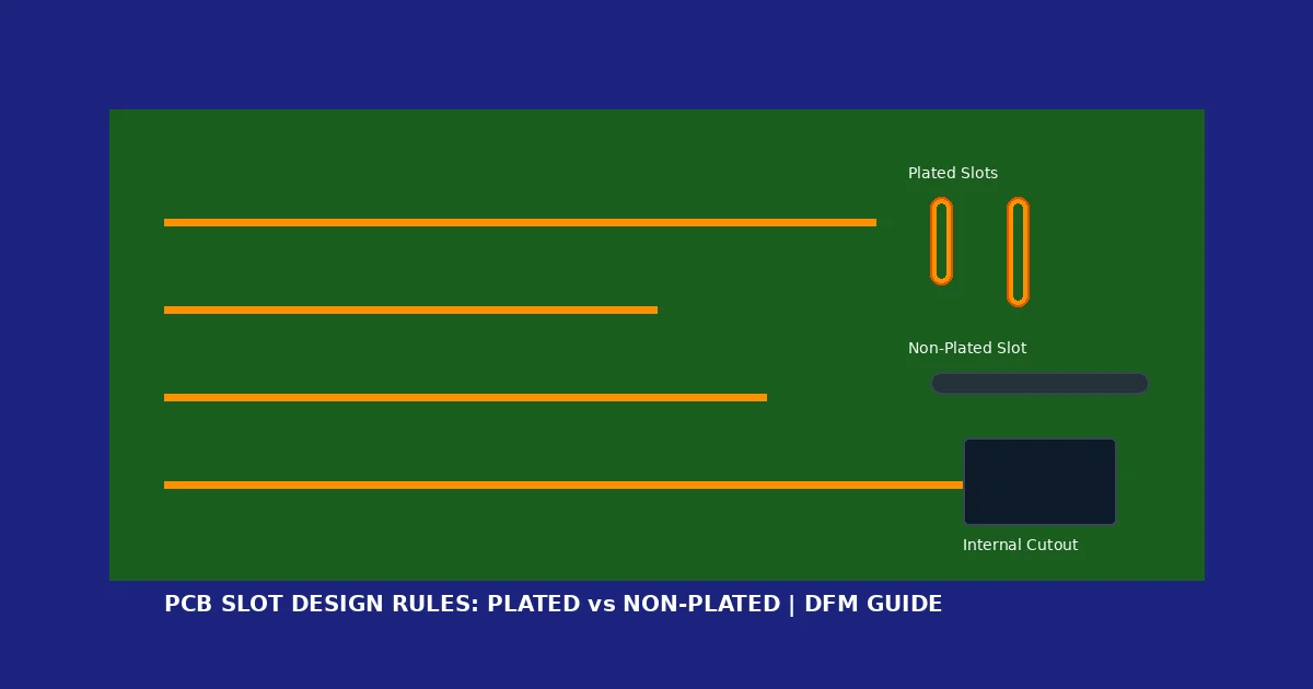
For non-plated through-holes (NPTH), tolerances are significantly tighter because no material is deposited after drilling. Standard NPTH tolerance is ±0.05 mm (±2 mil), achievable with standard CNC drilling equipment. For press-fit applications where the hole-to-pin interference fit is critical, tolerances of ±0.025 mm (±1 mil) are achievable but require dedicated tooling, controlled drill wear management, and 100% inspection — all of which carry cost premiums.
Position tolerance — how accurately the hole center lands relative to its designed coordinate — is equally critical. A perfectly sized hole shifted by 0.075 mm can break an inner-layer annular ring on a Class 3 design. Standard mechanical drilling achieves ±0.075 mm (±3 mil) position accuracy. Advanced processes with newer CNC equipment and optimized entry/exit material can tighten this to ±0.05 mm (±2 mil). Laser-drilled microvias achieve ±0.025 mm (±1 mil) position accuracy, which is one reason HDI designs can use such small pads with confidence.
The Complete Drill Size Selection Workflow: A Worked Example
Rather than presenting abstract rules, here is the exact workflow our engineers follow when reviewing a customer design that specifies a standard through-hole component on a multilayer board. This process ensures the finished hole will accommodate the component lead with appropriate clearance while maintaining reliable annular rings.
Design scenario: A 0.6 mm diameter round lead resistor mounted on a 1.6 mm thick, 6-layer board with ENIG surface finish, designed to IPC-6012 Class 2 requirements.
Step 1 — Determine maximum lead diameter. The component datasheet specifies lead diameter as 0.55 ±0.05 mm. Maximum lead diameter is therefore 0.60 mm. Always use the maximum material condition to ensure fit under worst-case conditions.
Step 2 — Add insertion clearance. For hand-soldered or machine-inserted components, standard practice adds 0.15-0.25 mm clearance beyond the maximum lead. We select 0.20 mm, giving a target finished hole size of 0.60 + 0.20 = 0.80 mm. This clearance allows components to drop into holes without force while being close enough for proper solder wetting.
Step 3 — Verify the finished hole is what you specify on the drawing. The fabrication drawing and drill table specify: “0.80 mm FINISHED, PLATED, ±0.10 mm.” You do not add plating compensation — the fabricator’s CAM department handles this. For ENIG, they will select a 0.90 mm drill tool.
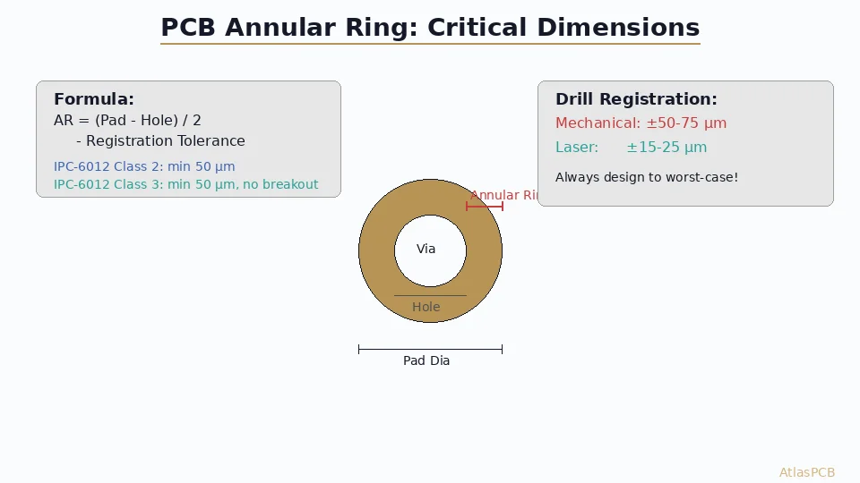
Step 4 — Verify the annular ring. With a 0.80 mm finished hole and standard tolerance of ±0.10 mm, worst-case finished hole diameter is 0.90 mm. If the pad diameter is 1.40 mm, the worst-case annular ring is (1.40 - 0.90) / 2 = 0.25 mm — well above the Class 2 allowance for 90-degree breakout and comfortably above the Class 3 minimum of 0.05 mm. Your design has margin.
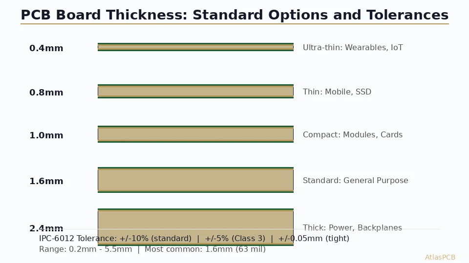
Step 5 — Check the aspect ratio. Board thickness is 1.6 mm. The fabricator’s drill tool is 0.90 mm. Aspect ratio = 1.6 / 0.90 = 1.78:1 — well within the standard 10:1 limit. No plating distribution concerns at this ratio.
Step 6 — Confirm position tolerance impact. With ±0.075 mm position tolerance, the annular ring minimum under combined worst-case (maximum hole + maximum position error) is 0.25 - 0.075 = 0.175 mm — still excellent for Class 2 and even Class 3.
This workflow takes sixty seconds for an experienced engineer but prevents the kinds of errors that add days to delivery schedules.
Let Our Engineers Verify Your Hole Specifications
Every order receives a complimentary DFM review where we check hole sizes, annular rings, aspect ratios, and tolerance feasibility against our production capabilities.
Upload Design FilesCommon Component Hole Sizing Reference
One of the most practical resources an engineer can have is a quick-reference table mapping common component lead sizes to appropriate finished holes and minimum pad sizes. The following values assume ENIG surface finish, Class 2 requirements, and standard plating thickness. For HASL boards, increase the finished hole by 0.05 mm to account for solder buildup:
Standard axial resistor leads (0.40-0.50 mm round): specify 0.70 mm finished hole with 1.20 mm minimum pad diameter. The fabricator drills 0.80 mm.
Standard axial capacitor and inductor leads (0.50-0.60 mm round): specify 0.80 mm finished hole with 1.40 mm minimum pad diameter. The fabricator drills 0.90 mm.
DIP IC leads (0.45 mm nominal, 2.54 mm pitch): specify 0.70 mm finished hole with 1.20 mm minimum pad diameter. The tight pitch means annular ring verification is important, especially on inner layers.
Standard 2.54 mm pitch pin headers (0.64 mm square post): the diagonal of a 0.64 mm square is 0.905 mm. Add 0.15 mm clearance above the diagonal maximum material condition, giving a finished hole of approximately 1.10 mm with 1.65 mm minimum pad. Square pins in round holes require careful attention — the diagonal, not the side dimension, determines the minimum opening.
Board-to-board connectors (1.0 mm round pins): specify 1.20 mm finished hole with 1.80 mm minimum pad. The fabricator drills 1.30 mm.
M2 mounting screws (clearance hole): specify 2.40 mm NPTH with ±0.05 mm tolerance. No plating allowance needed since the hole is non-plated. Clearance accommodates M2 screw diameter (2.0 mm) plus tolerance and plating on the screw.
M3 mounting screws (clearance hole): specify 3.40 mm NPTH with ±0.10 mm tolerance.
M4 mounting screws (clearance hole): specify 4.50 mm NPTH with ±0.10 mm tolerance. Holes this large are typically routed rather than drilled, which adds routing path tolerance.
Press-fit connector pins require special attention and are covered separately in our press-fit via design guide. These applications specify the hole tolerance to the connector manufacturer’s recommendation — typically ±0.025-0.05 mm NPTH — and cannot use the standard sizing approach above.
High Aspect Ratio: When Board Thickness Changes Everything
The aspect ratio of a drilled hole — defined as board thickness divided by drill diameter — directly affects how uniformly copper distributes along the barrel during plating. For standard aspect ratios below 8:1, modern plating processes deliver reasonably uniform barrel thickness from top to bottom. Above 8:1, the chemistry of electrolytic deposition changes the equation.
In a high aspect ratio hole, the electrolyte at the center of the barrel depletes faster than it can be refreshed through diffusion and convection. Current density drops at the barrel center while remaining higher at the top and bottom openings where fresh electrolyte is readily available. The result is a “dumbbell” distribution: thicker plating at the openings and thinner plating at the center. IPC-6012 addresses this by specifying both average and minimum plating thickness — the minimum is measured at the thinnest point, which is invariably the barrel center of high aspect ratio holes.
For a 2.4 mm thick 16-layer board with 0.25 mm finished vias, the fabricator drills 0.35 mm. The aspect ratio is 2.4/0.35 = 6.9:1 — manageable with standard chemistry. If the same board uses 0.20 mm finished vias, the drill becomes 0.30 mm and the ratio climbs to 8:1. Now the manufacturer needs pulse-reverse plating or extended plating cycles to achieve minimum barrel thickness at the center, adding cost and cycle time.
When aspect ratios exceed 10:1, most standard manufacturers cannot guarantee IPC-6012 Class 2 compliance without specialized equipment. If your design pushes this boundary, discuss it with your fabricator during the quoting stage — not after boards arrive with thin barrels that fail cross-section inspection. Our production line achieves reliable plating up to 12:1 for standard orders and 15:1 with premium process selection, but each step beyond 10:1 involves additional processing time and inspection that affects both cost and lead time.
The practical guidance: if your board is thicker than 2.0 mm, verify that your smallest via’s drill size keeps the aspect ratio below 10:1. If it cannot, either increase the via size (which uses more routing space), reduce the board thickness (which may affect impedance or mechanical requirements), or specify a manufacturer with high-aspect-ratio capability and budget for the premium.
How EDA Tools Export Drill Data
A persistent source of confusion is whether your EDA tool exports finished hole sizes or drill tool sizes in the Excellon drill file. The answer determines whether your fabricator receives the correct information or inadvertently double-compensates.
Altium Designer exports finished hole sizes by default. When you specify a 0.80 mm via in the footprint or schematic-driven layout, Altium writes 0.80 mm in the Excellon file. The fabricator’s CAM software reads this as the finished size and adds the appropriate plating compensation. This is the correct behavior for most workflows.
KiCad also exports finished hole sizes. The drill diameter entered in the footprint editor is the finished dimension that appears in the output drill file.
OrCAD/Allegro is configurable. Depending on the manufacturing output settings, Allegro can export either finished or fabrication (tool) sizes. Verify your output settings in the NC Drill parameters — and always cross-check by opening the generated drill file and comparing a known hole dimension against your design intent.
The safest practice regardless of EDA tool: include a general note on your fabrication drawing stating “ALL HOLE DIMENSIONS IN DRILL TABLE ARE FINISHED SIZES AFTER PLATING.” This eliminates ambiguity for the fabricator’s CAM engineer and prevents double-compensation errors. If for any reason your drill file specifies tool sizes instead of finished sizes, note explicitly: “DRILL SIZES IN EXCELLON FILE ARE TOOL DIAMETERS — FABRICATOR SHALL NOT ADD ADDITIONAL COMPENSATION.”
Cost Impact of Hole Tolerance Specifications
Tolerance specifications directly affect manufacturing cost, because tighter tolerances require more precise (and expensive) processes, increased inspection frequency, and lower yields. Understanding this relationship helps you specify appropriately — tight where functional requirements demand it, and standard everywhere else.
Standard tolerance (±0.10 mm for PTH, ±0.05 mm for NPTH) is included in base pricing with no surcharge. These tolerances are achievable with normal drill wear management, standard plating bath maintenance, and routine quality sampling. Approximately 90% of PCB orders fall entirely within standard tolerance requirements.
Tight tolerance (±0.05 mm for PTH, ±0.025 mm for NPTH) typically adds a 5-15% cost premium to the drilling and plating operations. The fabricator must use newer drill bits (reduced wear allowance before replacement), increase plating bath monitoring frequency, and inspect a larger sample of cross-sections to verify compliance. Lead time may extend by 1-2 days for the additional inspection steps.
Ultra-tight tolerance for press-fit connectors (±0.025 mm NPTH, often with ±0.025 mm position requirement) carries a 10-25% premium on the drilling operation. Every hole may require individual measurement with a pin gauge, and the drill bit replacement frequency increases dramatically. Some manufacturers dedicate specific spindles with newer bearings to press-fit work.
Position tolerance tightening from the standard ±0.075 mm to ±0.05 mm adds cost primarily through back-drill registration verification (X-ray or cross-section), more frequent registration coupon measurement, and reduced panel utilization (due to tighter registration acceptance windows).
The engineering decision: specify Class 3 and tight tolerances only on holes where the application genuinely requires it. A BGA via array on an inner layer needs Class 3 annular ring control. A through-hole LED mounting hole does not. Many designers apply Class 3 globally when only 5-10% of their holes need it — mixed-class callouts on the fabrication drawing save real money on production orders.
Optimize Your Hole Specifications for Cost and Reliability
Our engineering team reviews every order for tolerance feasibility. We flag unnecessarily tight specs that add cost without benefit and recommend optimized callouts that meet your functional requirements at lower price points.
Get an Instant QuoteHow to Specify Holes Correctly on Your Fabrication Drawing
The fabrication drawing is the contractual document that governs how your board is manufactured. Hole specifications that are clear, complete, and unambiguous prevent engineering queries and ensure the delivered boards match your design intent. Based on the most common EQ triggers we log, here is how to specify holes correctly:
Include a complete drill table with columns for: drill symbol, quantity, finished size, tolerance, plated or non-plated designation, and notes. Every unique hole size gets its own row. Vias and component holes should be distinguishable — either by separate drill symbols or by a “VIA” notation in the notes column. This allows the fabricator to apply different compensation rules to vias (where finished size is less critical) versus component holes (where assembly fit matters).
State the tolerance interpretation clearly. For component holes: “0.80 mm ±0.10 mm FINISHED PLATED.” For vias where exact finished size is non-critical: “0.30 mm +0.05/-drill diameter” — this tells the fabricator the design was checked with a 0.30 mm drill and the finished size may be anything up to 0.35 mm, giving them maximum latitude for yield optimization.
Call out the IPC class. A simple note — “BOARD SHALL CONFORM TO IPC-6012 CLASS 2” — sets the entire tolerance and quality framework. If specific holes need Class 3 treatment, note them individually: “PRESS-FIT HOLES (SYMBOL D3) SHALL MEET CLASS 3 REQUIREMENTS; ALL OTHERS CLASS 2.”
Specify the general fabrication note: “ALL DIMENSIONS ARE FINISHED SIZES AFTER PLATING UNLESS OTHERWISE NOTED.” This single sentence eliminates the most common source of drill size confusion between designer and manufacturer.
For non-standard requirements, provide explicit notes rather than relying on the fabricator to guess your intent. If a mounting hole must be plated for grounding but has a specific size requirement for a standoff, note both: “3.20 mm ±0.10 mm FINISHED PLATED — HOLE IS GROUNDED TO PLANES ON ALL LAYERS.” If a hole must remain unplated despite being surrounded by copper, call it out: “NPTH — DO NOT PLATE — MAINTAIN COPPER CLEARANCE PER KEEPOUT.”
When fabrication drawings are ambiguous, engineers ask questions. When they are clear, boards ship on schedule. Investing ten minutes in proper hole specification saves days of delay across a production year. For a comprehensive guide to all fabrication drawing requirements, see our PCB fab drawing checklist.
Avoiding the Most Expensive Hole-Related Mistakes
From our engineering review logs, the hole-related mistakes that generate the most costly delays follow predictable patterns. Understanding them helps you avoid the most common traps:
Mistake 1: Pre-compensating drill sizes in CAD. When a designer reads that plating removes 0.10 mm and manually adds 0.10 mm to every hole in their design, the fabricator’s CAM system adds another 0.10 mm on top. Every hole is now oversized by 0.10 mm, annular rings shrink by 0.05 mm per side, and the design may fail annular ring checks. The fix is simple: always specify finished sizes and let the fabricator compensate.
Mistake 2: Specifying ±0.025 mm tolerance on plated holes. This tolerance is physically unachievable for standard plated through-holes because the plating process alone introduces more variation than 0.025 mm. The engineering query delays the order while clarification is sought. Specify ±0.08 mm minimum for plated holes under 0.80 mm, and ±0.10 mm for holes 0.80 mm and above.
Mistake 3: Ignoring square pin diagonals. Designers specify holes for 0.64 mm square header pins using 0.64 + 0.20 = 0.84 mm finished hole size. But the diagonal of a 0.64 mm square is 0.905 mm — the hole is physically too small for the pin to enter. The correct calculation starts from the diagonal: 0.905 + 0.15 = approximately 1.05-1.10 mm finished hole.
Mistake 4: Same tolerance for all holes. Specifying ±0.05 mm tolerance globally when only press-fit holes need it wastes money. Standard vias and component holes perform perfectly at ±0.10 mm. Use mixed tolerances to control cost.
Mistake 5: Forgetting aspect ratio on thick boards. On a 3.2 mm board, a 0.25 mm finished via requires a 0.35 mm drill, creating a 9.1:1 aspect ratio that may exceed the manufacturer’s standard capability. The resulting thin barrel plating fails reliability testing. Check aspect ratios at the design stage, not after fabrication.
These five mistakes account for approximately 40% of all hole-related engineering queries our CAM department processes. Eliminating them from your design practice saves meaningful time and cost across every order you place.
Key Takeaways for Reliable Hole Specification
Specifying PCB holes correctly is not difficult once you understand the underlying manufacturing process. The finished hole size is what you specify in your CAD tool and on your fabrication drawing — it represents the usable opening on the delivered board. The fabricator selects the appropriate drill tool by adding compensation for copper plating and surface finish. Standard plated-hole tolerances of ±0.10 mm accommodate normal manufacturing variation without cost premiums, while tighter tolerances serve specific applications like press-fit connectors at additional cost. Component hole sizing starts from the maximum lead dimension plus insertion clearance, not from the nominal lead size. Aspect ratio verification prevents reliability issues on thick boards with small vias. And above all, clear fabrication drawing documentation — with explicit tolerance callouts, IPC class designation, and a “finished sizes” note — prevents the engineering queries and delays that erode your development schedule.
For engineers who want their boards manufactured correctly the first time, proper hole specification is one of the highest-leverage DFM practices available. Combined with appropriate annular ring design, aspect ratio awareness, and complete fabrication drawing documentation, it forms the foundation of trouble-free PCB procurement.
Ready to Order with Confidence?
Get an instant quote with free DFM review. Our engineers verify hole specifications, annular rings, and tolerance feasibility before production begins — ensuring your boards arrive right the first time.
Get Your Instant QuoteReviewed by AtlasPCB Engineering Team
About AtlasPCB — We specialize in complex PCB manufacturing for HDI, RF, and high-reliability applications. Explore our free engineering DFM review, or get an full PCB manufacturing capabilities . Every order includes free engineering review. Get your quote.
Reviewed by AtlasPCB Engineering Team — IPC-certified manufacturing specialists with 15+ years of production experience in HDI, RF, and high-reliability PCB fabrication. Content based on factory floor data and real customer design reviews.
- PCB drill size
- finished hole size
- plating allowance
- PCB hole tolerance
- DFM
- IPC-6012
- fabrication drawing
- annular ring