· AtlasPCB Engineering · Engineering · 10 min read
PCB DFM Check for Rigid-Flex Designs: Bend Zone, Coverlay, and Layer Transition Rules
Complete DFM checklist for rigid-flex PCBs covering bend zone copper routing, coverlay adhesion requirements, stiffener overlap tolerances, and the transition zone failures that account for 60% of rigid-flex manufacturing rejects.
Quick Answer
The three most common rigid-flex DFM failures are: vias placed within 1.0mm of the flex boundary (causes cracking), traces routed parallel to the bend axis (fatigue failure after 10-50 cycles), and insufficient stiffener overlap (delamination under thermal cycling). A proper DFM check catches these before fabrication.
Quick Answer: Top 5 Rigid-Flex DFM Failures
| Rank | DFM Error | Frequency | Consequence | Fix |
|---|---|---|---|---|
| 1 | Traces parallel to bend axis | 35% of rejects | Fatigue crack in 10-50 cycles | Route perpendicular to bend |
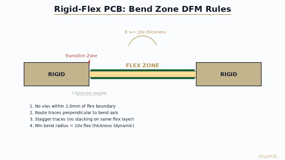
| 2 | Vias within 1.0mm of flex boundary | 25% of rejects | Cracking at transition | Move vias 1.0mm+ into rigid zone |
| 3 | Insufficient coverlay overlap | 15% of rejects | Copper exposure, corrosion | Minimum 0.25mm overlap on pads |
| 4 | Stacked traces (same XY on multiple flex layers) | 12% of rejects | Double stress concentration | Stagger traces between layers |
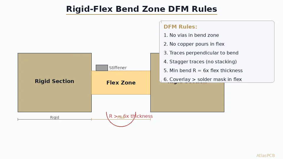
| 5 | Bend radius below minimum | 8% of rejects | Immediate or early-life crack | Dynamic: 10x thickness; Static: 6x |
These five issues account for approximately 95% of rigid-flex manufacturing rejects in our facility. Every single one is preventable with proper DFM review before fabrication begins.
The Transition Zone: Where Rigid-Flex PCBs Fail
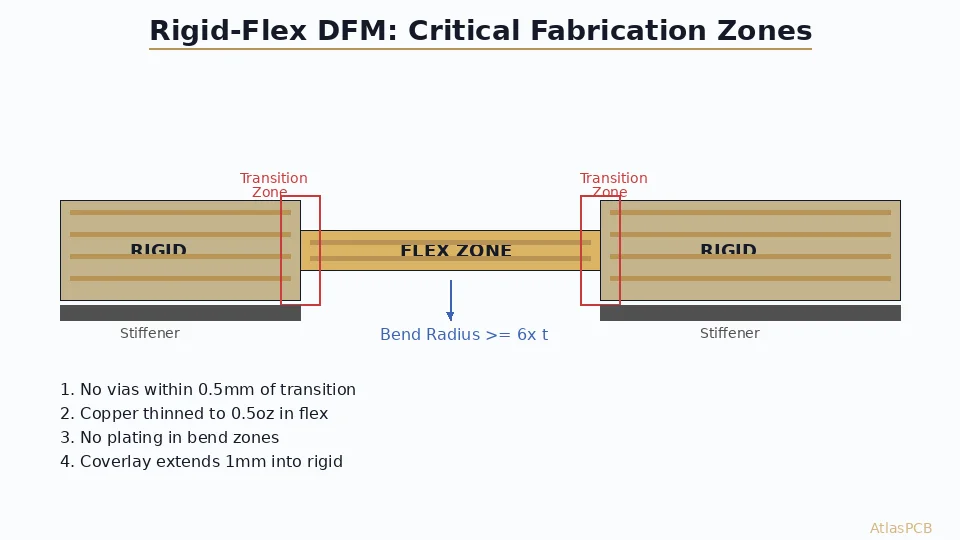
The most critical region in any rigid-flex design is not the flex section itself — it is the transition zone where rigid layers terminate and flex layers continue. This narrow boundary (typically 0.5-1.5mm wide) experiences the highest mechanical stress concentration during bending because it is the point where the full bending moment transitions from being distributed across the rigid stackup to being carried by only the thin flex layers.
In our production data from the past 24 months covering over 400 rigid-flex designs, approximately 60% of field failures originate in this transition region. The failure mechanism is straightforward: during each flex cycle, the transition zone acts as a stress riser because the abrupt change in stiffness creates a strain concentration factor of 2.5-4x compared to the center of the flex zone. This is analogous to a fatigue notch in mechanical engineering — and needs the same design attention.
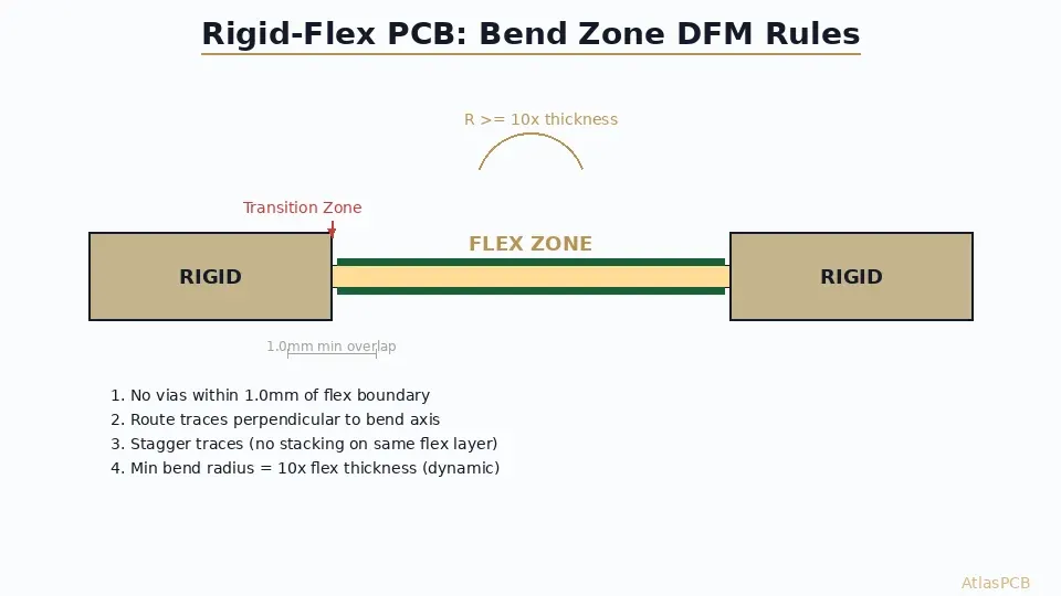
The three design features that protect the transition zone are: stiffener overlap (minimum 1.0mm of rigid laminate extending past the last via/pad), trace release (no sharp copper features within 0.5mm of the boundary), and gradual layer termination (stepping down layers rather than ending all rigid layers at the same XY coordinate). We enforce all three during our standard DFM review for any rigid-flex PCB order.
RIGID-FLEX DFM REVIEW
Catch Flex Zone Errors Before Fabrication
Upload your rigid-flex design for engineering review. We check bend radius, transition zones, via placement, and coverlay rules against IPC-2223 requirements.
Upload for DFM Review >
Bend Zone Copper Routing Rules
Copper trace routing in the flex bend zone follows a different set of rules than rigid PCB routing. The fundamental principle: copper traces in a bend zone experience cyclic tensile and compressive stress, and their survival depends on minimizing stress concentration while maximizing the number of available fatigue cycles before crack initiation.
Rule 1: Route perpendicular to the bend axis.
This is the single most important routing rule for rigid-flex reliability. When a trace runs perpendicular to the bend axis (crossing the bend at 90 degrees), it experiences pure bending stress distributed evenly along its length. When a trace runs parallel to the bend axis, it experiences concentrated tensile stress on the outer surface that is 3-5x higher than the perpendicular case. Our failure analysis data shows that parallel traces crack after 10-50 dynamic flex cycles, while perpendicular traces on the same board survive 100,000+ cycles.
If your routing requires traces to travel along the flex direction (parallel to bend), the trace must exit the bend zone into the rigid section before changing direction. Never turn a trace within the bend zone itself.
Rule 2: Stagger traces between flex layers — never stack.
For 2+ layer flex constructions, designers often route traces on adjacent layers at the same XY coordinates (directly on top of each other). This creates a locally thicker copper stack that acts as a stress concentration point. The correct approach: offset traces on adjacent layers by at least 1 trace width. This distributes the bending stress more evenly across the flex cross-section.
In practice, we recommend using odd-layer-only routing in flex zones when possible. A 2-layer flex with traces only on L1 and ground pour on L2 is significantly more reliable than traces on both layers, because the neutral bending axis passes through the adhesive layer between them rather than through the copper.
Rule 3: No trace width changes in the bend zone.
Any width transition (taper, necking, or pad flare) creates a stress concentration that accelerates fatigue. If your trace must connect to a different-width feature, make that transition at least 0.5mm inside the rigid section. The same applies to teardrops — while teardrops improve mechanical reliability in rigid boards, they create stress risers in flex zones and should not be used there.
Rule 4: Curved traces only — no acute angles.
All direction changes within the flex zone must use curved routing with a minimum radius of 1.5mm. Right-angle bends or 45-degree miters that are acceptable on rigid boards create immediate crack initiation points under flex stress. Most modern EDA tools support arc routing — use it throughout the flex zone without exception.
Coverlay Specification and Placement
Coverlay (polyimide film + adhesive laminate) serves the same protective function in flex zones that solder mask provides on rigid boards — but with the critical difference that it must survive millions of flex cycles without cracking, delaminating, or exposing copper to environmental corrosion.
The DFM parameters for coverlay that we check on every rigid-flex design entering our fabrication queue:
Coverlay material selection:
- Standard: 25um polyimide + 25um acrylic adhesive (50um total) — suitable for dynamic flex
- High-flex: 12.5um polyimide + 12.5um adhesive (25um total) — for tight bend radius applications
- Thick: 50um polyimide + 50um adhesive (100um total) — for environmental protection without flexing
Overlap requirements:
- Coverlay must overlap copper pads by minimum 0.25mm on all sides
- Coverlay opening registration tolerance: +/-0.1mm (laser cut) or +/-0.15mm (mechanical punch)
- Coverlay edge must extend at least 0.5mm past the last copper feature into the rigid boundary zone
- No coverlay openings (exposed pads) should exist within the bend zone — all pads must be in rigid zones
Adhesive flow control:
- During lamination, coverlay adhesive flows and fills spaces between traces
- Minimum trace spacing for reliable adhesive fill: 0.15mm (6 mil)
- If traces are closer than 0.15mm, trapped air creates adhesive voids that propagate delamination under flex
- Our process engineering team uses controlled-flow adhesive systems that reliably fill 0.10mm gaps, but 0.15mm provides manufacturing margin
A common designer mistake: specifying solder mask over the flex zone “for cost savings.” Solder mask is a brittle epoxy film that cracks on the first flex cycle, exposing copper traces to oxidation and potential short circuits from solder mask debris. We flag and reject this in DFM review — coverlay is mandatory for any flex zone that bends, even once during installation.
RIGID-FLEX MANUFACTURING
Rigid-Flex from 2 to 22 Layers
We fabricate rigid-flex PCBs with up to 12 flex layers and 22 total layers. Dynamic flex rated to 100,000+ cycles. IPC-6013 Class 3 certified.
Rigid-Flex Capabilities >Complete DFM Checklist: Before Submitting Your Rigid-Flex Design
Use this checklist before sending your rigid-flex Gerber files to any manufacturer. These items represent the complete set of checks our engineers perform during DFM review, organized by severity (critical failures first):
Critical (will cause fabrication failure or immediate field failure):
- Bend radius meets minimum: dynamic 10x, static 6x flex thickness
- No vias within 1.0mm of any rigid-to-flex boundary
- No traces routed parallel to bend axis in flex zones
- Coverlay specified (not solder mask) on all flex surfaces
- Stiffener/rigid overlap minimum 1.0mm past boundary
- No plated through-holes spanning the rigid-flex boundary
- Layer stackup clearly defines which layers continue into flex zones
High (causes yield loss or reduced reliability):
- Traces staggered between flex layers (not stacked vertically)
- No trace width changes within 0.5mm of flex zone
- Minimum trace spacing in flex zone: 0.15mm for adhesive flow
- Coverlay overlap on pads: minimum 0.25mm
- Curved routing only in flex zone (no angles less than 135 degrees)
- No copper pour/fill in flex bend zones (adds stiffness, reduces flexibility)
- Hatched ground on flex layers only (not solid pour)
Medium (affects cost or manufacturability):
- Flex layer count minimized (fewer layers = more flexible = longer life)
- Panelization allows flex sections to remain flat during processing
- Bookbinder construction specified for multi-flex-zone designs
- Strain relief features at connector/component transition points
- Test coupon includes flex endurance verification
For a detailed guide on the PCB DFM review process including how we handle DFM feedback and design iterations, see our comprehensive DFM article.
PCB DFM CHECK
Free DFM Feedback Within 24 Hours
Upload your rigid-flex design — our engineers review bend zones, transition areas, and coverlay spec against IPC-2223. DFM report delivered before quoting.
Upload Design Files >Real-World Case: Wearable Medical Device Rigid-Flex Rescue
A medical device customer came to us with a 6-layer rigid-flex design for a patient monitoring wearable (3 rigid zones, 2 flex zones). Their previous manufacturer had delivered 200 units with 38% field failure rate within 3 months — all trace cracks in the primary flex zone connecting the sensor module to the main processor board.
Our failure analysis revealed three compounding DFM errors in their original design:
- Power traces (0.3mm width, 2oz copper) routed parallel to the bend axis for 12mm through the flex zone — the primary failure mode
- Signal traces stacked on both flex layers at identical XY positions — doubling effective thickness and halving fatigue life
- Bend radius of 4mm on a 0.22mm flex section (18x ratio looked adequate, but 2oz copper has significantly lower fatigue life than 1oz)
Our engineering team redesigned the flex zone routing: power traces rerouted perpendicular with wider turn into the rigid zone, signal traces staggered by half-pitch between layers, and copper reduced to 1oz in flex zones with width compensation to maintain current capacity. The redesigned boards have been in the field for 14 months with zero flex-related failures across 1,500 units.
The lesson: rigid-flex DFM is not just about meeting minimum specifications — it is about understanding how multiple parameters interact. A bend radius that meets the “6x” static rule can still fail if the copper weight, trace orientation, and layer stacking create compound stress concentrations.
ATLASPCB
Rigid-Flex Done Right the First Time
Our engineering team reviews every rigid-flex design for bend zone compliance before fabrication begins. Upload your files — we will identify any DFM issues and suggest corrections.
Get DFM Review >
Reviewed by AtlasPCB Engineering Team — 15+ years in advanced PCB fabrication for RF, HDI, and rigid-flex applications.
Related Reading:
About AtlasPCB — We specialize in complex PCB manufacturing for HDI, RF, and high-reliability applications. Explore our rigid-flex PCB manufacturing, free engineering DFM review, or get an full PCB manufacturing capabilities . Every order includes free engineering review. Get your quote.
Reviewed by AtlasPCB Engineering Team — IPC-certified manufacturing specialists with 15+ years of production experience in HDI, RF, and high-reliability PCB fabrication. Content based on factory floor data and real customer design reviews.
Frequently Asked Questions
What is the minimum bend radius for a rigid-flex PCB?
Can I put vias in the flex section of a rigid-flex PCB?
How should traces be routed in rigid-flex bend zones?
What is coverlay and why does it matter for rigid-flex?
How much does a rigid-flex DFM error cost to fix?
- PCB DFM check
- rigid-flex PCB manufacturer
- rigid-flex DFM
- bend zone design
- flex PCB manufacturing