· AtlasPCB Engineering Team · Engineering · 18 min read
PCB Design-for-Assembly (DFA): Component Placement, Orientation, and Spacing Rules That Prevent Assembly Defects
A comprehensive DFA guide covering component placement strategies, orientation conventions, spacing requirements, and keep-out zones that reduce assembly defects, improve pick-and-place yields, and lower production costs in volume PCB manufacturing.
Quick Answer
PCB Design-for-Assembly (DFA) ensures that component placement, orientation, and spacing follow standardized rules that maximize automated assembly yield, minimize rework, and reduce overall production cost. Key principles include maintaining consistent component orientation, providing adequate spacing between parts for pick-and-place nozzles, observing keep-out zones near board edges and mounting holes, and designing pad geometries that prevent tombstoning, bridging, and solder insufficiency during reflow.
Why Design-for-Assembly Matters More Than Most Engineers Realize
Every PCB engineer understands that a circuit must function electrically. Far fewer appreciate that a board’s physical layout determines whether it can be assembled reliably, affordably, and at scale. Design-for-Assembly is the discipline that bridges this gap — transforming a working schematic capture into a production-ready layout that automated equipment can process without error.
The stakes are substantial. A single tombstoned 0402 capacitor on a 2,000-unit production run does not simply cost the price of one capacitor. It triggers optical inspection flags, manual rework station time, potential damage to adjacent components from rework heat, and re-inspection overhead. Multiply that by the dozens of potential defect modes that poor DFA creates, and assembly costs can easily exceed bare board fabrication costs by an order of magnitude.
At AtlasPCB, our engineering review team evaluates hundreds of designs monthly before they enter our fabrication lines. The patterns we observe are remarkably consistent: engineers who follow systematic DFA rules from the earliest layout stages achieve first-pass assembly yields above 99.5%, while designs that ignore these principles routinely suffer 3-5% defect rates that consume margin and delay shipments.
This guide distills the component placement, orientation, and spacing rules that our fabrication and assembly engineering teams have validated across thousands of production builds. These are not theoretical recommendations — they reflect the actual capabilities and constraints of modern high-speed pick-and-place equipment, reflow ovens, and automated optical inspection systems.
Reviewed by AtlasPCB Engineering Team
Component Orientation: The Foundation of Efficient Assembly
Component orientation is perhaps the most underestimated aspect of PCB layout. Engineers often place parts wherever routing convenience dictates, without considering the downstream implications for automated assembly. This approach creates layouts that technically work but dramatically increase programming complexity, placement time, and error probability.
The Single-Axis Rule for Passive Components
All two-terminal passive components (resistors, capacitors, inductors) should align to a single axis wherever physically possible. On a typical board, this means orienting all 0402 and 0603 passives with their long axis parallel to the board’s X-axis or Y-axis — not a mixture of both. When a layout uses a consistent orientation, the pick-and-place machine can process entire groups of components without rotation corrections, reducing cycle time and eliminating angular placement errors.
The practical reality of modern pick-and-place equipment is that each component rotation adds a small but measurable time penalty and introduces potential angular error. For a 12-mil-pitch 0201 component, even a 2-degree rotation error can result in insufficient solder paste coverage on one pad. By eliminating unnecessary rotations through consistent orientation, you remove this error source entirely.
Where two orientations are unavoidable (complex routing sometimes demands it), group components by orientation into distinct board regions. This allows the placement program to process all 0-degree parts in one pass and all 90-degree parts in another, maintaining efficiency while accommodating routing constraints.
Polarized Component Alignment
For polarized components — electrolytic capacitors, diodes, transistors, ICs — establish a consistent convention and maintain it across the entire design. The most common and recommended convention is:
Pin 1 or the cathode mark should face the same board edge (typically top or left) for all components of a given type. When this is impossible due to routing, limit the number of unique orientations to two rather than allowing arbitrary angles. Every additional orientation variant increases the probability of placement error during programming and production verification.
This consistency serves multiple purposes beyond assembly. During visual inspection, technicians can rapidly verify correct orientation by scanning rows of identically-aligned parts. During rework, the orientation convention eliminates confusion about proper component direction. And during test, systematic orientation patterns simplify probe access planning.
IC Placement Conventions
Integrated circuits — QFPs, BGAs, QFNs, and SOICs — deserve particular attention to placement conventions. For QFP and SOIC packages, orient all devices with pin 1 in the upper-left corner when viewed from the component side. This convention aligns with IPC-7351B land pattern standards and ensures that the majority of available component library definitions will not require rotation adjustments.
For BGA components, pin A1 orientation should be consistent across all BGAs on the board. When mixing BGA pitch classes (0.4 mm, 0.5 mm, 0.65 mm, 0.8 mm, 1.0 mm), group similar pitches together on the board to simplify placement verification. Fine-pitch BGAs below 0.5 mm pitch require local fiducial marks at diagonal corners — ensure that fiducial placement does not conflict with the component’s own keep-out requirements.
Spacing Requirements: Room to Breathe, Room to Build
Component spacing rules exist at the intersection of three constraints: pick-and-place nozzle clearance, reflow soldering physics, and post-assembly inspection access. Violating any one of these constraints creates defects, but engineers often optimize for only electrical function and routing density without considering the physical realities of the assembly process.
Minimum Body-to-Body Clearance
The fundamental spacing constraint comes from pick-and-place nozzle geometry. Modern high-speed placement machines use vacuum nozzles that extend beyond the component body perimeter during pickup and placement. If adjacent components are too close, the nozzle physically interferes with already-placed parts, causing displacement, rotation errors, or outright collision damage.
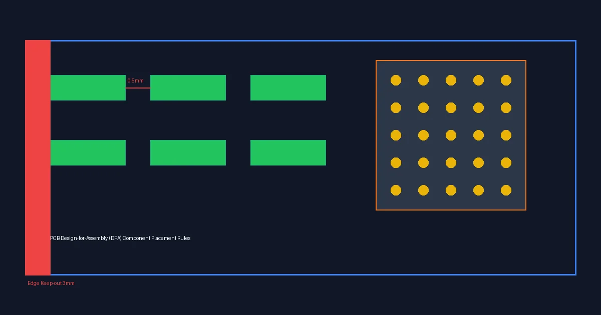
For standard passive components (0402 and larger), maintain minimum 0.5 mm clearance between component bodies — not between pad edges, but between the physical outlines of the placed parts. For components smaller than 0402 (0201, 01005), many contract manufacturers require 0.3 mm minimum but strongly prefer 0.5 mm for reliable high-speed placement.
Between active IC packages, spacing requirements increase substantially. A QFP-144 with 0.5 mm lead pitch requires at least 1.5 mm clearance from its lead tips to any adjacent component body. This clearance ensures that the placement nozzle does not disturb the QFP during adjacent part placement and provides adequate inspection access for post-reflow AOI cameras.
Tall components present a unique challenge. Any component exceeding 3 mm in height creates a “shadow zone” that can block solder paste deposition on adjacent pads during stencil printing, interfere with pick-and-place nozzle approach angles, and create thermal shadowing during reflow that results in insufficient solder melting. Maintain minimum 2.0 mm clearance from tall component bodies, increasing to 3.0 mm on the reflow oven’s downstream side where thermal shadowing is most severe.
Through-Hole Component Spacing
Through-hole components in a mixed-technology assembly (where most parts are SMD but selected connectors, transformers, or power devices use through-hole mounting) require additional spacing consideration. The protruding leads on the bottom side must not interfere with bottom-side SMD components, and the component bodies must provide adequate clearance for selective soldering or wave-soldering processes.
For selective soldering access, maintain a minimum 2.5 mm clearance between through-hole component leads and adjacent SMD component bodies on the bottom side. The selective solder nozzle requires this clearance to approach the through-hole joint without transferring heat to neighboring SMD solder joints. Where wave soldering is used (increasingly rare but still common for high-pin-count connectors), maintain 5.0 mm clearance in the wave direction.
BGA Escape Routing and Component Proximity
BGA components present a compound spacing challenge. The ball grid extends to within a few hundred microns of the package edge, requiring via fan-out patterns that consume substantial board area around the package perimeter. When placing components adjacent to BGAs, account for both the package body and the via fan-out region.
For a 0.8 mm pitch BGA, the dog-bone escape pattern typically extends 1.5-2.0 mm beyond the package edge before traces can route to inner layers. No component should be placed within this escape region. Effectively, the minimum placement distance from a BGA package edge to an adjacent component is approximately 3.0-4.0 mm for standard-pitch BGAs and 2.0-2.5 mm for fine-pitch BGAs using via-in-pad technology that eliminates the dog-bone fan-out.
Keep-Out Zones: Protecting Assembly Integrity
Keep-out zones define regions where no component may be placed, regardless of available space. These zones protect against mechanical damage during manufacturing, ensure proper equipment engagement during assembly processing, and maintain adequate clearance for board-level testing.
Board Edge Keep-Out
The board edge keep-out is the most frequently violated DFA rule we encounter in design reviews. Engineers see unused board area near edges and fill it with decoupling capacitors or termination resistors, unaware that these components will be damaged during panel routing, stressed during depaneling, or lost entirely when V-score separation occurs.
For routed board edges (tab-routed panels), maintain a minimum 3.0 mm keep-out from the board outline to any component body. This clearance accounts for router bit radius, board flexion during routing, and debris generation that can contaminate solder joints. For V-scored edges, the minimum reduces to 1.0 mm because V-score separation generates less mechanical stress, but components placed this close to V-score lines must be limited to low-profile parts (under 1.5 mm height) to prevent stress fractures during panel break.
Rail edges — the panel border strips that engage with conveyor rails during reflow — require the most generous keep-out. Maintain 5.0 mm minimum from rail edges to any component, as this region is gripped by mechanical rails that would crush any protruding part. Most panel designs place the rails outside the individual board outlines, so this constraint primarily affects panel border components in panelized assemblies.
Mounting Hole and Tooling Hole Keep-Out
Mounting holes and tooling holes (used for fixturing during assembly and testing) create keep-out requirements that extend well beyond the hole diameter itself. For a standard M3 mounting hole (3.2 mm drill), the keep-out radius should extend 3.5 mm from the hole center to any component body. This accounts for washer and nut dimensions during final mechanical assembly, plus the press-fit tooling pins that engage these holes during selective soldering and in-circuit testing.
Tooling holes for automated fixturing typically require 2.5 mm keep-out radius. These holes are used by the pick-and-place machine’s board support pins and by the AOI system’s board clamping mechanisms. Components placed within this zone risk being crushed by support pins or creating false inspection failures due to partial occlusion by clamp mechanisms.
Connector and Edge-Mounted Device Keep-Out
Edge-mounted connectors (USB, HDMI, Ethernet, board-to-board) require dedicated keep-out zones on their mating face. No component may be placed within the connector’s mating envelope plus 1.0 mm clearance. This seems obvious, but we frequently see engineers place decoupling capacitors within 0.5 mm of a USB-C connector’s mating face, where they either interfere with cable insertion or are damaged by insertion force.
Additionally, tall edge-mounted connectors create “reflow shadow” zones on their board-side face. Components placed immediately behind a tall connector body may not achieve adequate reflow temperature because the connector’s thermal mass acts as a heat sink. Maintain minimum 2.0 mm clearance between tall connector bodies and adjacent temperature-sensitive SMD joints.
Preventing Common Assembly Defects Through Design
The majority of assembly defects are preventable through intelligent board layout. While solder paste quality, reflow profile optimization, and placement accuracy all contribute to yield, the PCB design itself determines the theoretical maximum yield achievable with perfect process control. A poorly designed board cannot be saved by excellent equipment.
Tombstoning Prevention
Tombstoning — where a passive component stands up on one end during reflow — is the most common SMD defect attributed to poor design rather than poor process. The physics are straightforward: surface tension forces from molten solder pull the component toward the pad with greater wetting. If the forces are asymmetric between the two pads, the component lifts on the weaker side.
Design-level tombstoning prevention focuses on ensuring thermal and solder-volume symmetry between component pads. The most common design violation is connecting one pad of a passive component directly to a large copper plane (ground or power) while the other pad connects only to a trace. The plane-connected pad has enormously greater thermal mass, causing the solder to melt later on that side. While the trace-connected pad’s solder is already molten (creating surface tension), the plane-connected pad is still solid, creating the force imbalance that lifts the component.
The solution is thermal relief on any pad connecting to a large copper area. Standard thermal relief patterns (four spokes connecting the pad to the plane through narrow traces) equalize the heating rate between pads. For critical components (timing references, precision voltage dividers), consider routing both pads through identical trace lengths to equalize thermal paths completely.
Additionally, orient small passive components (0402 and smaller) perpendicular to the board’s reflow direction. In a convection reflow oven, temperature gradients exist along the conveyor travel direction. Components oriented parallel to this direction expose their two pads to slightly different temperatures at any given instant, while perpendicularly-oriented components present both pads to the same thermal zone simultaneously.
Solder Bridging Prevention
Solder bridging between adjacent pads occurs when excess solder or insufficient solder mask dam creates a conductive path between isolated conductors. While stencil design and solder paste volume control are the primary defenses, PCB design plays a critical role in establishing the physical barriers that prevent bridging.
The solder mask dam — the strip of solder mask material between adjacent pads — must be wide enough to survive the mask application process and maintain its integrity during reflow. For standard LPI (Liquid Photo-Imageable) solder mask, the minimum dam width is 75 μm (3 mil). However, this is an absolute minimum that represents the process capability limit. Design for 100 μm (4 mil) minimum dams to provide manufacturing margin.
For fine-pitch QFP and connector leads (0.5 mm pitch and below), solder mask dam integrity becomes critical. At 0.5 mm pitch with typical 0.3 mm pad width, the dam between pads is only 0.2 mm — barely above the 75 μm minimum when pad definition tolerances are considered. For these components, specify solder-mask-defined (SMD) pads rather than non-solder-mask-defined (NSMD) pads, which provides more precise pad geometry control and wider effective dams.
Insufficient Solder (Dry Joint) Prevention
Insufficient solder results from inadequate paste volume reaching the pad-component interface. While primarily a stencil design issue, PCB layout creates conditions that exacerbate paste insufficiency. The most common design-driven cause is excessive via-in-pad solder drainage, where unfilled vias beneath component pads wick solder away from the joint during reflow.
When via-in-pad is required (unavoidable for fine-pitch BGAs and certain QFNs), specify VIPPO (Via-In-Pad Plated Over) with complete fill and planarization. Unfilled or tent-only vias beneath component pads will drain solder during reflow, creating voided or insufficient joints that fail reliability testing. This is particularly critical for BGA pads, where solder drainage into unfilled vias directly reduces ball height and creates void-prone joints that fail thermal cycling.
Test Access Design: Planning for In-Circuit Testing
Design-for-test (DFT) requirements intersect heavily with DFA rules, and engineers often discover test access conflicts only after assembly tooling has been built. Planning test point placement during initial layout prevents expensive redesigns and enables in-circuit testing (ICT) that catches assembly defects before functional testing.
Test Point Placement Rules
Every net requiring ICT verification needs a dedicated test point — a small exposed copper pad (typically 0.9-1.0 mm diameter) accessible from one board side. Place test points on a regular grid spacing (2.54 mm or 1.27 mm grid) to simplify bed-of-nails fixture design. Avoid placing test points within 1.0 mm of component bodies, as fixture probe alignment tolerances could cause probe-to-component interference.
For double-sided boards, concentrate test points on the bottom side (opposite the primary component side) whenever possible. This allows the fixture to access test points while components face upward for visual inspection and rework access. When bottom-side test access is impossible due to bottom-side components, plan for flying-probe testing with adequate clearance (1.5 mm minimum between test points) for probe tip access.
Test Point Keep-Out From Board Support
During in-circuit testing, the board rests on support pins that prevent flexion when test probes apply downward force. These support pin locations require keep-out zones — no test points, vias, or components should be placed where support pins contact the board. Typical support pin diameter is 2.5 mm, requiring 3.5 mm keep-out circles at each support location.
Communicate with your assembly partner early in the design phase to determine support pin locations. Many designers are surprised to learn that support pins are required at specific intervals (typically every 20-30 mm) across the board to prevent excessive flexion during test probe contact. These keep-out requirements can significantly constrain layout options if not planned from the start.
Thermal Considerations in Component Placement
Reflow soldering exposes the entire board assembly to elevated temperatures (typically 245-260°C peak for lead-free processes). The spatial arrangement of components directly affects local temperature distributions, which in turn affects solder joint quality and component reliability.
Thermal Mass Distribution
Large thermal mass components — QFPs, BGAs, transformers, electrolytic capacitors, heat sinks — absorb significant thermal energy during reflow and create local cool zones. Components placed immediately adjacent to these thermal masses may not achieve adequate peak temperature, resulting in cold joints or insufficient intermetallic formation.
Distribute high-thermal-mass components evenly across the board rather than clustering them in one region. When clustering is unavoidable (such as a processor BGA surrounded by decoupling capacitors), ensure that the reflow profile accounts for the thermal lag in this region and that adjacent small components are not placed in direct thermal shadow.
Double-Sided Reflow Component Weight
For double-sided SMT boards processed with two reflow passes (first side, then second side with the first side facing down), the second-pass reflow must not cause components on the first side to fall off due to gravity when their solder re-melts. Components exceeding the surface tension retention limit (approximately 30 grams per joint for standard pad geometries) must be placed on the second-pass side, or adhesive must be specified for first-side placement.
In practice, this means heavy connectors, large electrolytic capacitors, and high-mass inductors should all be on the same board side (processed second). Small passives, ICs, and low-mass components can safely be placed on either side. When a design requires heavy components on both sides, discuss adhesive application options with your assembler — but recognize that adhesive adds process cost and complicates rework.
Panel-Level DFA: Designing for Array Assembly
Production assemblies are rarely processed as individual boards. Panels containing multiple board images pass through assembly equipment as a single unit, and the panel design itself affects assembly yield. Engineers who design only the individual board without considering panelization create avoidable problems during production.
Panel Fiducial and Break-Away Tab Considerations
Panel-level global fiducials must be placed on the panel rails, not on individual boards. Individual boards should contain their own local fiducials for fine-alignment correction, but the panel fiducials provide the gross alignment reference for the entire array.
Break-away tabs connecting individual boards within a panel must be strong enough to survive assembly handling (conveyor transport, stencil printing pressure, component placement forces) without separation, yet weak enough to allow clean depaneling without board damage. Standard mouse-bite tabs (3-5 drill holes of 0.5-0.6 mm diameter) provide this balance when spaced at 50-80 mm intervals along board edges.
Place no components within 1.0 mm of break-away tabs. During depaneling, flexion stress radiates approximately 1.0 mm from the separation point. Components placed within this zone experience mechanical stress that can crack solder joints, fracture ceramic capacitor bodies, or damage BGA ball arrays.
DFA Checklist for Production Release
Before releasing a design to manufacturing, verify each of these DFA requirements against your specific layout:
The component orientation should follow a consistent convention throughout the design, with passive parts aligned to primary axes and ICs oriented with pin 1 in a common direction. Body-to-body clearances should meet or exceed the minimum spacing for each component class — 0.5 mm for standard passives, 1.5 mm adjacent to fine-pitch ICs, 2.0 mm near tall components. Board edge keep-out zones of 3.0 mm from routed edges and 5.0 mm from rail edges should be free of all components.
Thermal relief patterns should be present on all pads connecting to copper planes, particularly for small passive components susceptible to tombstoning. Via-in-pad usage should specify VIPPO fill and planarization. Solder mask dams between fine-pitch pads should be verified at 100 μm minimum width. Test points should be accessible from one board side and placed on a regular grid with adequate clearance from components and support pin locations.
The panel design should include proper fiducials, adequate break-away tab strength, and component keep-out zones near all depaneling features. Heavy components should be assigned to the second reflow side, and double-sided thermal mass distribution should be evaluated for adequate reflow temperature uniformity.
How AtlasPCB Supports Your DFA Optimization
Our engineering review process evaluates every design submission against comprehensive DFA criteria before fabrication begins. When we identify potential assembly issues — inadequate spacing, thermal symmetry violations, or test access limitations — we provide specific, actionable feedback with dimensional recommendations rather than generic rule violations.
For designs targeting high-volume production (1,000+ units), we offer complimentary DFA consultation during the quoting phase. This pre-fabrication review catches the issues that are inexpensive to fix in layout but extremely costly to resolve after tooling is built. Our assembly engineering team draws on experience from processing over 3,000 unique designs annually, giving us pattern-recognition capabilities that identify subtle DFA issues before they manifest as production defects.
Whether you are designing a prototype board for initial validation or preparing a production-ready layout for volume manufacturing, systematic DFA practices reduce risk, accelerate time-to-market, and protect your unit economics. The rules in this guide represent the accumulated manufacturing knowledge that separates first-time-right designs from costly iterative redesigns.
About AtlasPCB — We specialize in complex PCB manufacturing for HDI, RF, and high-reliability applications. Explore our PCB assembly services, free engineering DFM review, or get an full PCB manufacturing capabilities . Every order includes free engineering review. Get your quote.
Reviewed by AtlasPCB Engineering Team — IPC-certified manufacturing specialists with 15+ years of production experience in HDI, RF, and high-reliability PCB fabrication. Content based on factory floor data and real customer design reviews.
Frequently Asked Questions
What is the minimum spacing between SMD components for automated assembly?
Why does component orientation matter in PCB assembly?
What keep-out distance is required from PCB edges for components?
How do I prevent tombstoning defects through PCB design?
- PCB DFA
- design for assembly
- component placement
- pick-and-place
- SMT assembly
- DFM
- PCB manufacturing