· AtlasPCB Engineering Team · Engineering · 13 min read
PCB Copper Weight Selection: Cost Impact of 2oz vs 3oz vs 4oz Outer Layers
Understand how heavy copper weight selection affects PCB fabrication cost, including etching yield, drill wear, plating time, material premiums, and practical strategies to optimize cost without sacrificing current-carrying capacity.
Why Copper Weight Is the Largest Single Cost Driver in Power PCBs
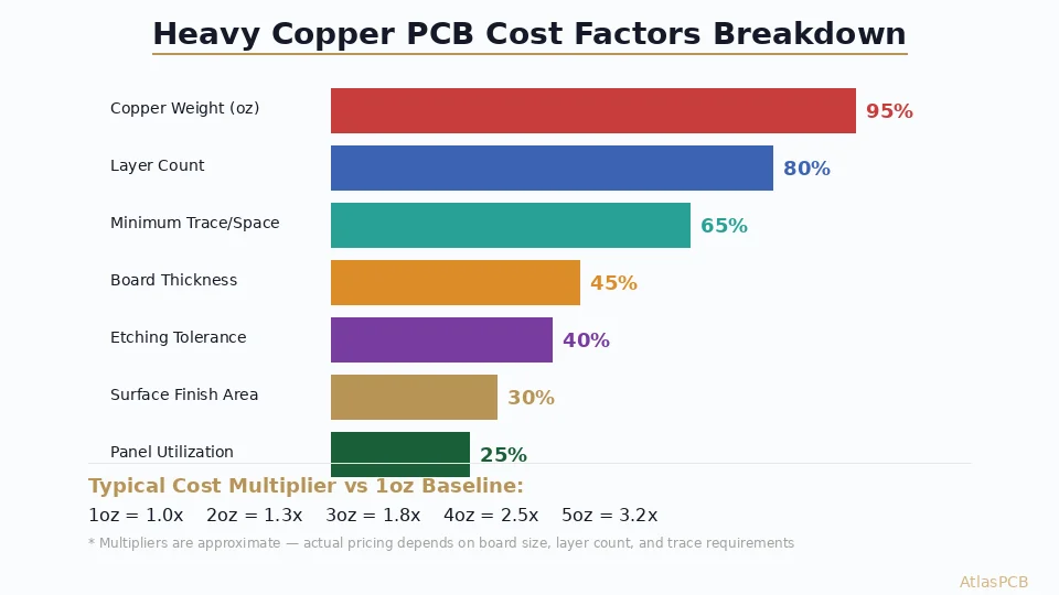
Every PCB designer understands that adding layers increases board cost. What many designers underestimate is the equally dramatic cost impact of increasing copper weight on existing layers. Moving from standard 1oz copper to 2oz on outer layers typically adds 15 to 25 percent to fabrication cost. Stepping up to 3oz adds 40 to 60 percent. And specifying 4oz outer layers can double the base fabrication price compared to an otherwise identical 1oz design. These are not arbitrary markups—they reflect genuine manufacturing complexity increases that compound across multiple process steps.
Understanding why heavy copper costs more enables designers to make informed tradeoffs between copper weight, trace width, board area, and total product cost. In many cases, a design that initially specifies 3oz copper can achieve identical electrical performance with 2oz copper and modest trace width increases, saving substantial fabrication cost without any functional compromise. This article explains the cost mechanisms, provides practical comparison data, and offers design strategies that our engineering team recommends to clients optimizing power delivery designs for production economics.
How Copper Weight Translates to Physical Thickness
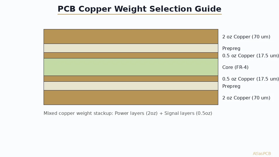
Before discussing cost impacts, establishing the relationship between copper weight specifications and physical copper thickness provides essential context. The copper weight system originated in the foil manufacturing industry, where weight per unit area defines thickness. One ounce copper refers to a copper foil weighing one ounce per square foot, which corresponds to approximately 35 micrometers or 1.4 mils thickness. This relationship scales linearly: 2oz equals 70 micrometers, 3oz equals 105 micrometers, and 4oz equals 140 micrometers.
These are the starting foil thicknesses on outer layers. After the plating process adds approximately 25 to 35 micrometers of additional copper to the surface during through-hole plating, the finished copper thickness on outer layers exceeds the base foil weight. A board starting with 2oz foil finishes at roughly 95 to 105 micrometers total outer copper thickness—effectively approaching 3oz finished thickness on the outer surfaces. This distinction between starting foil weight and finished copper thickness matters when calculating current-carrying capacity and thermal dissipation.
Inner layers do not receive additional plating copper, so inner layer thickness equals the specified foil weight. A 2oz inner layer remains 70 micrometers throughout processing. This difference means that current-carrying requirements can sometimes be met with lighter outer copper (which gets plated up) while using heavier inner copper where needed for power planes.
Cost Factor One: Base Material Premium
The first cost increase begins before any fabrication process starts—in the raw material itself. Copper-clad laminate pricing scales with copper foil thickness because thicker foil requires more copper per unit area and thicker foil is more difficult to manufacture uniformly.
For standard FR-4 laminate, the material cost premium follows an approximately linear relationship with copper weight. Compared to 1oz base material, 2oz laminate costs approximately 20 to 30 percent more per panel. The 3oz material adds 50 to 70 percent to material cost, and 4oz laminate costs roughly double the 1oz equivalent. These percentages fluctuate with copper market pricing—during the current period of elevated copper costs driven by AI server demand, the premiums have widened further.
The material premium affects every layer where heavy copper is specified. A six-layer board with 2oz on all layers pays the premium six times, while a board with 2oz only on outer layers pays it twice. This creates a clear cost optimization opportunity: use heavy copper only on the specific layers that require it for electrical performance, keeping signal layers at standard 1oz or even half-ounce weights.
Cost Factor Two: Etching Complexity and Yield
Copper etching is the process that defines trace geometry by removing unwanted copper between circuit features. Thicker copper requires longer etch times, stronger chemistry, and produces wider undercut—the lateral erosion beneath the photoresist that narrows traces beyond their designed width. This undercut phenomenon is the single largest manufacturing challenge associated with heavy copper fabrication.
For standard 1oz copper, the etch undercut is approximately equal to the copper thickness—35 micrometers of lateral erosion on each side of a trace. This is well understood and easily compensated in standard design rules. At 2oz copper, the undercut increases to approximately 50 to 70 micrometers per side due to the longer etch time required. By 3oz, undercut reaches 80 to 110 micrometers, and 4oz copper produces 100 to 140 micrometers of lateral erosion.
This undercut directly constrains minimum trace width and spacing. While 1oz copper readily produces 75 micrometer (3 mil) traces and spaces, 2oz copper requires minimum trace widths of 150 micrometers (6 mils) to remain after undercut compensation. Three-ounce copper pushes minimum features to 200 micrometers (8 mils), and 4oz typically requires 250 to 300 micrometers (10 to 12 mils) minimum. Designers who specify heavy copper without adjusting their minimum features discover during DFM review that their fine-pitch routing is incompatible with the copper weight they have selected.
The yield impact extends beyond geometry. Longer etch times increase the probability of defects—open circuits from over-etching, shorts from under-etching, and surface quality issues from uneven etch distribution across the panel. Our production data shows that outer layer etching yield for 1oz copper consistently exceeds 98 percent. At 2oz, yield drops to approximately 95 percent. Three-ounce copper produces yields around 90 to 92 percent, and 4oz outer layers see yields of 85 to 90 percent. These yield reductions translate directly to cost because fabricators must start more panels to achieve the same quantity of good boards.
Cost Factor Three: Drilling and Via Formation
Mechanical drilling through heavy copper wears drill bits faster, requires slower feed rates, and demands more frequent bit changes. Copper is significantly harder on carbide drill bits than the surrounding dielectric, and each additional ounce of copper that the drill must penetrate adds wear equivalent to approximately 0.2 mm of additional board thickness.
For a standard multilayer board with 1oz copper on all layers, drill bit life is typically 3000 to 5000 hits depending on hole diameter and board thickness. At 2oz copper on outer layers, bit life decreases by approximately 20 percent. With 3oz outer copper, bit life drops 35 to 40 percent, and 4oz outer copper reduces bit life by roughly half. The additional bit changes add time to the drilling process and increase consumable costs that factor directly into board pricing.
Via reliability also enters the equation. Thicker copper at the drill entry and exit points creates larger burrs that require more aggressive deburring, and the plating must bridge a greater step height at the via knee—the transition from barrel wall to surface pad. Inadequate plating coverage at this high-stress location leads to via fatigue failure during thermal cycling. Fabricators compensate by extending plating times and adding process controls, both of which add cost.
For boards exceeding 3oz outer copper, our standard process includes an additional mechanical deburring step followed by plasma desmear treatment to ensure clean hole walls before plating. This extra process step adds approximately 8 to 12 percent to processing time on the drilling and preparation line.
Cost Factor Four: Plating Process Time
Electroplating copper into drilled vias and onto panel surfaces operates at a controlled deposition rate—typically 20 to 25 micrometers per hour for conventional acid copper plating. While all boards receive the same plating time regardless of starting copper weight (the plating adds to existing thickness uniformly), heavy copper boards require additional attention during the plating process.
The primary challenge is achieving uniform plating distribution between the thick outer surfaces and the thin via barrels. Standard plating produces a thickness ratio called throwing power—the ratio of barrel copper to surface copper. For standard boards, a throwing power of 0.7 to 0.8 is acceptable. Heavy copper boards with deep, high-aspect-ratio holes require enhanced throwing power achieved through specialized plating chemistry, pulse plating, or extended low-current-density cycles. These process modifications add time and chemistry costs.
Additionally, heavy copper outer layers require more aggressive surface preparation before plating to ensure adhesion. The thicker copper develops a more tenacious oxide layer during processing that must be completely removed through extended microetch cycles. Inadequate preparation leads to copper delamination during thermal excursion, which is the second most common reliability failure mode we observe in heavy copper production.
Cost Factor Five: Solder Mask Application
Applying solder mask uniformly over heavy copper topography is substantially more challenging than masking standard boards. The step height between copper traces and adjacent bare laminate is 70 micrometers for 2oz, 105 micrometers for 3oz, and 140 micrometers for 4oz. Solder mask must fill these valleys completely while providing minimum coverage over copper peaks, and the mask thickness must be sufficient to prevent exposure of copper edges during handling and assembly.
Standard solder mask application through screen printing or curtain coating deposits 20 to 30 micrometers of mask over copper surfaces. For 1oz copper, this provides adequate coverage with standard processes. For 2oz and above, multiple mask application cycles may be required to fill the trace valleys adequately—a technique called double-print or plug-and-print that approximately doubles the solder mask processing time.
An alternative approach used for 3oz and heavier copper is to specify thicker solder mask materials designed for high-copper applications. These materials cost more per unit volume and require modified exposure and development parameters, but they can be applied in a single pass. The choice between multiple thin passes and single thick passes depends on feature density—fine-pitch areas may not tolerate the thicker material’s reduced resolution capability.
Comparative Cost Summary
Combining all cost factors produces the following approximate relationship between copper weight and total fabrication cost for a representative six-layer board with heavy copper on outer layers only, remaining layers at 1oz, standard FR-4 material, and 0.8 mm minimum features:
Starting from a 1oz baseline, specifying 2oz outer layers increases total board fabrication cost by approximately 18 to 25 percent. The increase reflects material premium, moderate yield reduction, slightly faster drill wear, and standard solder mask processing. This remains within the “standard” pricing tier at most fabricators, including our own.
Moving to 3oz outer layers increases cost by 40 to 60 percent over the 1oz baseline. This represents a category change in manufacturing complexity—the board enters our heavy copper production routing with additional process controls, slower etching, more drill changes, and potentially double-print solder mask. Lead times typically extend by 2 to 3 working days.
Four-ounce outer layers add 80 to 120 percent to the baseline cost, effectively doubling the fabrication price. At this copper weight, every process step requires modified parameters, yields drop measurably, and the board often requires engineering disposition for minor cosmetic issues that would be rejectable on standard product. Lead times extend by 5 to 7 working days minimum.
Strategies to Reduce Heavy Copper Cost
Experienced designers employ several techniques to achieve the current-carrying performance of heavy copper without the full cost penalty. These strategies have been validated through thousands of production designs at our facility.
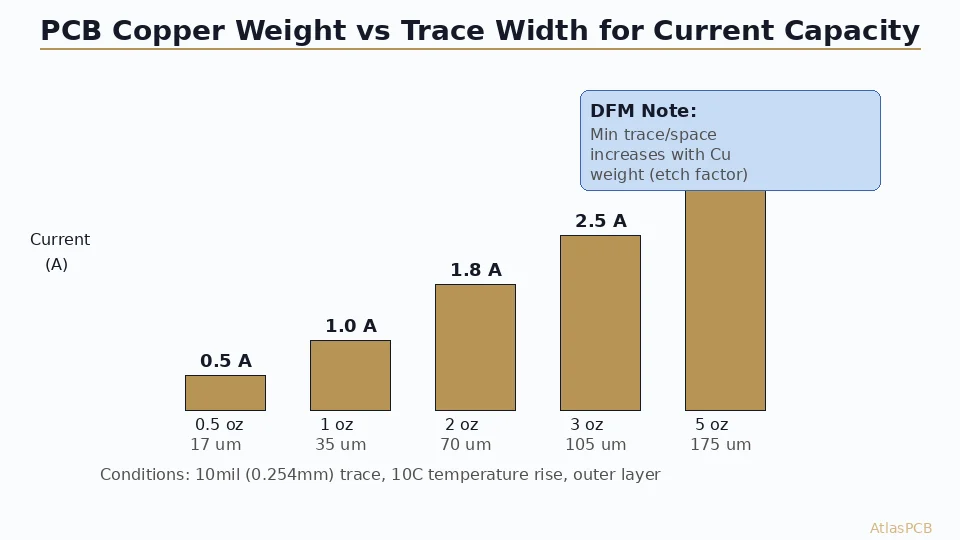
The most effective strategy is widening traces rather than thickening copper. Current-carrying capacity scales linearly with both width and thickness, meaning a 2oz copper trace at 2 mm width carries identical current to a 4oz copper trace at 1 mm width. Since the cost of wider traces is essentially free (requiring only board area), any design with available routing space should maximize trace width before increasing copper weight. Our engineering team routinely identifies opportunities during DFM review where trace widths can increase by 50 to 100 percent without impacting other routing, eliminating the need for the heavier copper originally specified.
Using heavy copper selectively—only on specific layers—reduces material and processing costs. Power delivery designs often require heavy copper only on dedicated power and ground planes while maintaining standard 1oz copper on signal routing layers. This hybrid approach costs significantly less than specifying heavy copper uniformly while delivering identical power handling performance. A board with 3oz inner power planes and 1oz outer signal layers costs roughly 30 percent less to fabricate than the same design with 3oz on all layers.
Thermal relief optimization reduces the total copper area that must be etched at heavy weight. Rather than flooding entire planes with solid copper, using thermal relief patterns around non-power vias reduces the effective copper coverage to 60 to 70 percent while maintaining power delivery capability. Less copper to etch means faster processing, better yield, and lower cost.
Considering via current capacity alongside trace current capacity sometimes reveals that the vias—not the traces—are the current bottleneck. In such cases, adding more vias in parallel rather than increasing copper weight provides more effective current distribution. Multiple 0.3 mm vias in 1oz copper often outperform a single via in 3oz copper for both current capacity and thermal dissipation.
When Heavy Copper Is Genuinely Required
Despite cost optimization strategies, certain applications genuinely require heavy copper weight that cannot be substituted with wider traces or more vias. High-current power electronics driving motors, inverters, or welding equipment routinely require 60 to 200 amperes through board-level conductors, where even maximum-width traces in 2oz copper cannot provide sufficient cross-sectional area.
Thermal management applications where copper serves as a heat spreader rather than purely as a conductor also benefit from heavy copper. The thermal conductivity of copper at 385 watts per meter-kelvin makes thick copper layers effective heat spreaders when positioned directly beneath power devices. In these applications, the copper weight selection is driven by thermal resistance calculations rather than current capacity, and reducing weight means reducing thermal performance.
High-reliability applications with extreme thermal cycling—automotive under-hood, aerospace, or downhole drilling electronics—may specify heavy copper to provide sufficient fatigue margin over decades of thermal cycling. Thicker copper barrel walls in vias and thicker surface traces resist fatigue crack propagation longer than thin copper under cyclic thermal strain. For these applications, the heavy copper cost premium buys reliability margin that cannot be achieved through alternative means.
Making the Cost-Optimal Selection
The decision process for copper weight selection should follow a structured engineering analysis rather than defaulting to “heavier is better.” Begin with the electrical requirements: calculate maximum continuous current and peak current for each net, then determine the minimum copper cross-section using IPC-2152 charts or thermal simulation. Compare this minimum cross-section against what each copper weight provides at your available trace widths.
If 2oz copper at achievable trace widths provides adequate current margin with at least 50 percent derating, stop there—2oz represents the optimal cost-performance balance for the majority of power applications. If calculations show 2oz is insufficient even at maximum trace width, move to 3oz and repeat the analysis. Reserve 4oz for applications where 3oz genuinely cannot meet requirements after all geometric optimization has been exhausted.
At AtlasPCB, we include copper weight optimization as part of our standard DFM review for every power board quotation. When our engineers identify opportunities to reduce copper weight without compromising electrical performance, we present the alternative specification alongside the cost savings. This collaborative approach has saved clients significant fabrication cost while maintaining full performance compliance—typically achieving 20 to 40 percent cost reduction compared to the initial heavy copper specification.
Reviewed by AtlasPCB Engineering Team
Need a Cost-Optimized Heavy Copper PCB Quote?
Our engineering team analyzes your current requirements and recommends the most cost-effective copper weight specification. Get pricing for 2oz, 3oz, and 4oz options compared side-by-side.
Get a QuoteAbout AtlasPCB — We specialize in complex PCB manufacturing for HDI, RF, and high-reliability applications. Explore our heavy copper PCB manufacturing, or get an free engineering DFM review . Every order includes free engineering review. Get your quote.
Reviewed by AtlasPCB Engineering Team — IPC-certified manufacturing specialists with 15+ years of production experience in HDI, RF, and high-reliability PCB fabrication. Content based on factory floor data and real customer design reviews.
- heavy copper PCB
- copper weight
- PCB cost
- 2oz copper
- 3oz copper
- 4oz copper
- current capacity
- DFM