· Thomas Webb · Engineering · 13 min read
PCB Design Considerations for GaN Power Modules: Thermal and Layout Challenges
A fabrication and layout engineering guide to designing PCBs for gallium nitride power modules, addressing thermal via strategies, copper weight selection, creepage requirements, parasitic inductance minimization, and laminate choices for GaN's unique switching characteristics.

Gallium nitride power devices have transitioned from laboratory curiosities to mainstream components in power electronics, now appearing in everything from laptop chargers and server power supplies to electric vehicle onboard chargers and solar inverters. GaN’s ability to switch at frequencies five to ten times higher than silicon MOSFETs while maintaining low on-resistance enables dramatically smaller magnetics, reduced passive component count, and higher power density. However, these advantages come with PCB design and fabrication demands that differ significantly from traditional silicon-based power converter design. The combination of extreme switching speeds (voltage slew rates exceeding 100 V/ns), concentrated heat flux from small die areas, and sensitivity to parasitic circuit elements creates a design environment where PCB layout and material selection directly determine whether the GaN device achieves its potential or destroys itself in operation.
Understanding GaN’s Unique Demands on the PCB
Traditional silicon power MOSFETs switch at rates of 5 to 20 V/ns in typical applications, giving the designer relatively relaxed requirements for loop inductance, trace routing, and ground plane integrity. GaN high-electron-mobility transistors (HEMTs) routinely achieve slew rates of 50 to 150 V/ns, with some emerging devices capable of 200 V/ns or more. This ten-fold increase in switching speed compresses the switching transition time from tens of nanoseconds to single nanoseconds, making the PCB’s parasitic inductance the dominant factor determining voltage overshoot, electromagnetic interference, and switching loss.
The relationship between loop inductance and voltage overshoot is described by V = L(di/dt), where the inductance of the power loop directly multiplies the rate of current change during switching. For a GaN half-bridge switching 20 amperes in 2 nanoseconds (di/dt = 10 A/ns), even 1 nanohenry of loop inductance generates 10 volts of overshoot. With GaN devices typically rated at 650 volts with absolute maximum ratings of 700 to 750 volts, every nanohenry of excessive loop inductance consumes safety margin that the designer cannot afford to waste. Achieving total power loop inductances below 1 nanohenry demands PCB layout techniques that are fundamentally different from those used in silicon MOSFET designs.
The thermal challenge is equally demanding but in a different dimension. GaN devices achieve high power density partly because their die areas are much smaller than equivalent silicon devices. A 650V/30A GaN HEMT might occupy a die area of 4 by 6 millimeters, dissipating 3 to 5 watts of switching and conduction loss during normal operation. This concentrated heat flux — often exceeding 30 W/cm-squared at the package interface — must be conducted through the PCB to reach the heatsink or ambient environment. The thermal path through the board becomes a critical design element rather than an afterthought.
Power Loop Layout for Minimum Inductance
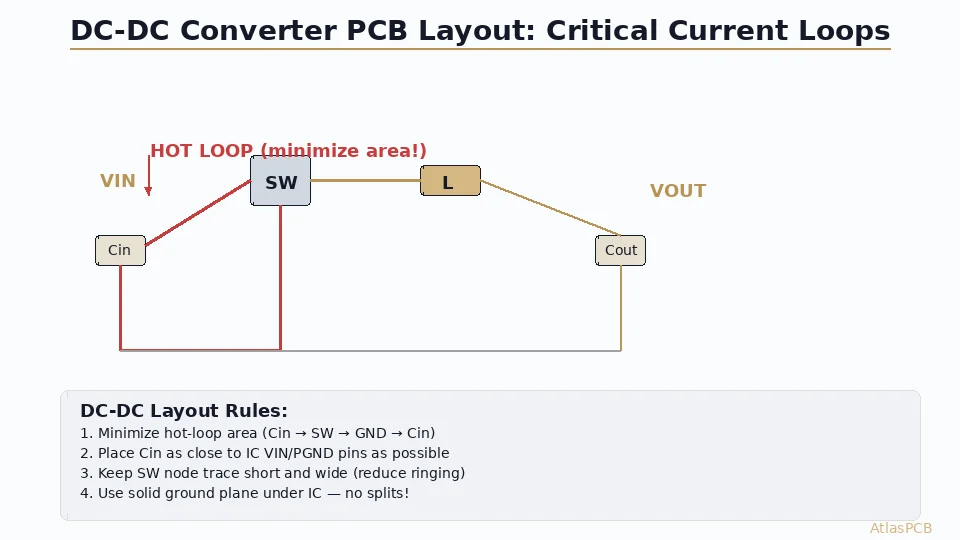
The fundamental principle for minimizing power loop inductance in a PCB layout is maximizing mutual coupling between the forward and return current paths. When forward current flows in one direction on a given layer and return current flows in the opposite direction on an adjacent layer directly above or below, their magnetic fields partially cancel, reducing net loop inductance. This principle drives the requirement for extremely tight vertical coupling between the power switching node and the DC bus decoupling.
In practice, this means placing the high-side and low-side GaN devices as close together as physically possible, with the decoupling capacitors positioned within millimeters of the device power terminals. The power loop should complete its circuit vertically through the board thickness rather than horizontally across the board surface. A properly optimized half-bridge power stage for GaN places the bus decoupling capacitors directly opposite the GaN devices on the bottom side of the board, creating a power loop that circulates through a vertical cylinder of minimal diameter. The forward current path through the high-side device connects to the midpoint on the top layer, while the return path from the decoupling capacitor completes through vias and the adjacent ground layer with minimal horizontal displacement.
Our fabrication experience with GaN power converter boards reveals that the most successful designs use 4-layer or 6-layer stackups with the following layer assignment philosophy: Layer 1 carries the power components and switching node copper; Layer 2 serves as a solid ground reference plane directly below the power stage; Layers 3 and 4 (in a 4-layer design) carry power distribution and auxiliary circuitry. The critical design parameter is the dielectric spacing between Layer 1 and Layer 2. Thinner dielectric provides tighter coupling and lower inductance but also lower voltage standoff capability. For 650V GaN applications, a dielectric spacing of 0.2 to 0.3 millimeters between the power layer and ground plane provides a good balance between inductance minimization and insulation requirements.
The specific copper features connecting the GaN device pads to the decoupling capacitors must be treated as transmission line structures rather than simple interconnect. Trace widths should be as wide as physically possible — ideally filling the entire available area between the component pads — to minimize resistive loss and distribute current uniformly. Sharp corners should be avoided in the power loop because they create current crowding that increases effective resistance and generates localized electromagnetic field concentrations.
Thermal Via Design and Copper Weight Strategy
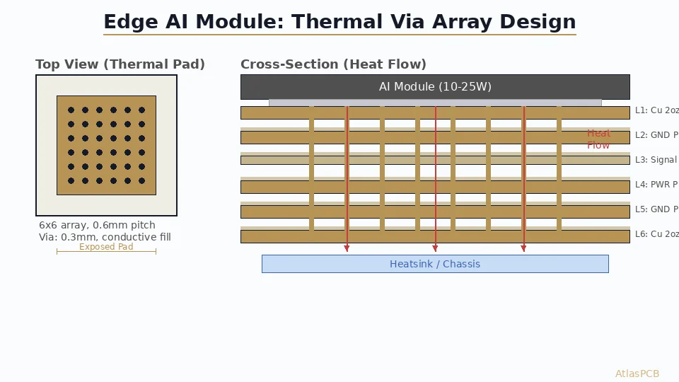
GaN devices in power modules typically feature exposed thermal pads on their bottom surface that serve simultaneously as the primary heat extraction path and the electrical connection to the source or drain potential. The PCB must conduct this heat vertically through the board to a heatsink mounted on the opposite side or to a large copper pour that dissipates heat through convection and radiation.
Thermal vias provide the vertical heat conduction path. For a thermal pad area of 5 by 5 millimeters typical of many GaN power modules, we recommend filling this area with as many vias as design rules permit. Using 0.3 millimeter drilled vias on 0.6 millimeter pitch (center to center), a 5 by 5 millimeter pad area accommodates approximately 49 to 64 thermal vias. Each via, with 25 micrometers of copper plating on its walls, provides a thermal conductance of approximately 0.8 to 1.0 W/K depending on board thickness. The array of 50 to 60 vias in parallel provides total thermal conductance of 40 to 60 W/K — sufficient to maintain acceptable temperature rise for 3 to 5 watts of dissipation through the board.
For higher power applications dissipating 10 watts or more per device, standard plated-through vias alone cannot provide adequate thermal conductance. In these cases, we recommend one of two enhanced approaches: filled and plated-over vias (VIPPO) that allow solder to flow into the via barrels during reflow, creating solid copper-solder thermal columns; or copper coin insertion, where a solid copper slug is press-fit or bonded into a milled cavity directly below the thermal pad, providing thermal conductivity an order of magnitude higher than via arrays.
Copper weight selection on the power layers significantly impacts both current-carrying capacity and thermal spreading. Standard 1-ounce (35 micrometer) copper is insufficient for most GaN power applications. We recommend 2-ounce (70 micrometer) copper on the power layer as a minimum, with 3-ounce (105 micrometer) or 4-ounce (140 micrometer) copper preferred for designs carrying continuous currents above 15 amperes. The heavier copper provides three benefits simultaneously: lower resistive loss in power traces, improved thermal spreading from hot spots to larger copper areas, and greater current-carrying margin during transient overload conditions.
From a fabrication perspective, heavy copper introduces manufacturing considerations that designers should anticipate. Etch factor increases with copper weight — 2-ounce copper requires wider trace spacing than 1-ounce copper to achieve the same isolation gap after etching. Our minimum trace spacing on 2-ounce copper is 0.15 millimeters compared to 0.10 millimeters for 1-ounce copper. At 3-ounce weight, minimum spacing increases to 0.20 millimeters. These spacing requirements must be factored into the layout from the beginning rather than discovered during DFM review after layout completion.
Creepage and Clearance for High-Voltage GaN
GaN power devices operating at 650 volts or higher introduce high-voltage isolation requirements that constrain PCB layout geometry. The relevant standards (IPC-2221, IEC 62368-1, UL 60950) specify minimum creepage distances (along surfaces) and clearance distances (through air) based on operating voltage, pollution degree, and material group. For 650V operation in pollution degree 2 environments (typical enclosed electronics), minimum creepage distances of 3.2 to 6.4 millimeters are common depending on the specific standard applied and the board’s comparative tracking index.
These creepage requirements profoundly impact the layout of GaN power stages because they mandate large keep-out zones between high-voltage nodes and low-voltage control circuits. The gate drive signals for GaN devices must cross this isolation boundary using either isolated gate drivers with integrated transformers or optocoupler-based isolation, with the PCB layout maintaining required creepage at all points along the isolation boundary.
In our fabrication experience, designers of GaN-based converters frequently request routed slots in the PCB between high-voltage and low-voltage domains to increase the effective creepage distance without enlarging the overall board dimensions. A 1 millimeter wide routed slot effectively doubles the creepage distance for a given physical separation because the surface path must travel down one side of the slot, across the bottom, and up the other side. We can fabricate slots as narrow as 0.8 millimeters using standard routing tooling, though 1.0 to 1.5 millimeters provides more robust fabrication margin.
Solder mask properties also factor into creepage calculations. Standard solder mask is typically classified as IEC Material Group IIIa or IIIb, which reduces required creepage distances compared to bare laminate surfaces. However, this requires the solder mask to remain intact and uncontaminated throughout the product’s service life — an assumption that may not hold in harsh environments with condensation, contamination, or mechanical abrasion. Conservative designs calculate creepage based on uncoated laminate distances and treat solder mask as an additional safety margin rather than a design enabler.
Laminate Selection for GaN Applications
The extreme switching speeds of GaN devices generate electromagnetic emissions that propagate through both conducted and radiated paths. The PCB laminate’s dielectric properties influence the propagation characteristics of these high-frequency emissions, and the laminate’s thermal properties determine how well the board handles concentrated heat flux from GaN devices.
For most GaN power converter applications below 1 MHz switching frequency, standard FR-4 (Tg 170C or higher) provides adequate electrical performance. The dielectric loss tangent of FR-4 at power conversion frequencies (100 kHz to 3 MHz) is low enough that substrate losses are negligible compared to device switching and conduction losses. The primary material consideration becomes thermal — ensuring the laminate’s glass transition temperature provides adequate margin above the expected PCB temperature in the thermal pad region.
For GaN converters operating at switching frequencies above 1 MHz or with particularly aggressive dv/dt requirements, mid-loss laminates such as Panasonic Megtron-4 or Isola IS680 offer improved high-frequency behavior and lower dielectric loss, which reduces substrate heating from high-frequency current harmonics flowing through the power planes. The cost premium of these materials (typically 20 to 40 percent above standard FR-4) is justified in designs where the thermal budget is extremely tight or where EMI emissions must be minimized to meet Class B radiated emissions requirements without external shielding.
Thermal conductivity of the laminate itself (typically 0.3 to 0.4 W/mK for standard FR-4) is generally insufficient to provide meaningful lateral heat spreading in the board plane. The dominant thermal paths are vertical (through copper planes and thermal vias) rather than lateral (through the dielectric). This means that copper pour area and via array design matter far more than laminate thermal conductivity for most designs. The exception arises in applications using insulated metal substrate (IMS) or metal-core PCBs, where an aluminum or copper base provides thermal conductivity of 1 to 4 W/mK — a ten-fold improvement that enables direct heatsink mounting without thermal vias.
Gate Drive Routing and Noise Immunity
The gate drive circuit for GaN devices requires careful PCB routing to maintain signal integrity in an environment dominated by high dv/dt and di/dt noise sources. GaN HEMTs typically have threshold voltages of 1.2 to 2.0 volts — significantly lower than silicon MOSFETs (4 to 6 volts) — making them highly susceptible to false turn-on from gate noise coupling. A few hundred millivolts of noise on the gate can cause momentary conduction, creating shoot-through conditions in half-bridge topologies that destroy both devices within nanoseconds.
The PCB layout must provide a dedicated, low-inductance gate drive loop that is physically separated from the power loop and shielded by ground copper from dv/dt-induced displacement currents. The gate drive traces should be routed as differential pairs (gate and source return) with minimal loop area, running directly adjacent to each other to maximize mutual inductance cancellation. The source return path for the gate drive must connect at the device’s Kelvin source pin (when available) rather than sharing the power source connection, which carries switching current transients that would couple directly into the gate circuit.
Ground plane partitioning in the region around GaN devices requires careful consideration. The power ground (carrying switching currents) and signal ground (referencing gate drives and control circuits) should ideally connect at a single point near the device source to prevent switching current from flowing through signal ground paths. This star-ground topology at the device level prevents common-impedance coupling that would inject switching noise into the gate drive and control loops.
Manufacturing and Assembly Considerations
GaN power modules often use QFN or LGA package styles with exposed thermal pads that require specific PCB pad design and solder paste stencil patterns to achieve void-free solder joints. Voids under thermal pads directly degrade thermal performance by blocking heat conduction paths, and large voids can cause solder fatigue cracking under thermal cycling.
Our recommended approach uses a segmented solder paste stencil design for thermal pads — dividing the large pad into multiple smaller paste deposits separated by narrow gaps. This segmentation allows entrapped flux gases to escape during reflow rather than being trapped under a continuous solder layer. Typical segmentation uses 1.0 to 1.5 millimeter paste squares separated by 0.3 millimeter gaps, achieving void content below 15 percent consistently in production. Some designers specify vacuum reflow for critical thermal joints, which can reduce void content below 5 percent but adds significant assembly cost.
Via-in-pad under GaN thermal pads requires either plugging the vias with epoxy fill and plating over (VIPPO process) or capping with solder mask to prevent solder wicking during reflow. Unfilled, uncapped vias under thermal pads act as solder sinks, pulling paste away from the pad surface and creating both voiding and insufficient solder volume for reliable joint formation. Our standard process for GaN power boards includes epoxy-filled and planarized vias in all thermal pad areas, ensuring flat pad surfaces for consistent paste printing and joint quality.
The tight spacing typical of GaN power stages — with high-voltage and low-voltage features separated by minimum creepage distances — demands precise solder paste registration during assembly. We recommend solder paste stencil aperture reductions of 10 to 15 percent on fine-pitch pads adjacent to isolation boundaries to prevent bridging across creepage gaps, and we verify paste registration accuracy to within 50 micrometers for all GaN power module footprints.
Reviewed by AtlasPCB Engineering Team
ATLASPCB POWER ELECTRONICS
Heavy Copper and Thermal Via Expertise for GaN Designs
We fabricate 2-oz to 6-oz copper boards with VIPPO thermal vias, routed isolation slots, and controlled impedance for demanding power electronics applications. Free DFM review included.
Get Power PCB Quote ›About AtlasPCB — We specialize in complex PCB manufacturing for HDI, RF, and high-reliability applications. Explore our heavy copper PCB manufacturing, aluminum and metal-core PCB services, or get an free engineering DFM review . Every order includes free engineering review. Get your quote.
Reviewed by AtlasPCB Engineering Team — IPC-certified manufacturing specialists with 15+ years of production experience in HDI, RF, and high-reliability PCB fabrication. Content based on factory floor data and real customer design reviews.
- GaN
- power electronics
- thermal management
- PCB layout
- power module
- DFM