· AtlasPCB Engineering Team · Engineering · 13 min read
ENIG vs ENEPIG Surface Finish: When to Use Each for BGA Reliability
A detailed comparison of ENIG and ENEPIG surface finishes for BGA reliability, covering black pad mitigation, solder joint strength, wire bonding compatibility, and cost considerations for high-reliability PCB assemblies.
The Surface Finish Decision That Determines BGA Reliability
When a design engineer specifies a ball grid array package with pitch below 0.5 mm, the choice of surface finish becomes one of the most critical decisions affecting long-term solder joint reliability. Both ENIG and ENEPIG have earned their place as premium surface finishes in the PCB industry, but they serve different reliability requirements that engineers must understand before committing to a fabrication specification. Having processed thousands of BGA-intensive boards through our production lines, we have developed clear guidelines for when each finish delivers optimal performance and when choosing the wrong one leads to field failures that could have been prevented at the design stage.
The fundamental distinction between these two finishes lies in a single additional metal layer that transforms the electrochemical behavior of the entire pad surface. ENIG deposits electroless nickel followed by a thin immersion gold layer, creating a solderable surface that has served the industry well for decades. ENEPIG adds an electroless palladium interlayer between the nickel and gold, creating a barrier that addresses the most persistent reliability concern in high-density packaging: the black pad phenomenon.
Understanding the Layer Structures
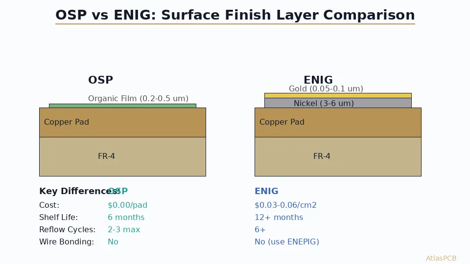
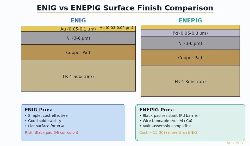
ENIG consists of two functional layers deposited onto the copper pad surface. The electroless nickel layer, typically 3 to 6 micrometers thick, provides the structural foundation and acts as a diffusion barrier between copper and tin during soldering. The immersion gold layer, ranging from 0.05 to 0.15 micrometers, protects the nickel from oxidation during storage and assembly. During reflow soldering, this thin gold dissolves almost instantly into the molten solder, exposing the underlying nickel to form the critical nickel-tin intermetallic compound that creates the mechanical bond.
ENEPIG introduces a palladium layer between 0.05 and 0.3 micrometers thick, positioned between the nickel and gold layers. This palladium interlayer serves multiple functions that become increasingly important as component packaging density increases. The palladium acts as a secondary diffusion barrier, provides an alternative bonding surface for wire bonding applications, and most importantly, fundamentally changes the gold deposition mechanism to eliminate the conditions that cause black pad.
The electrochemical difference matters enormously in practice. In the ENIG process, gold deposits through a galvanic displacement reaction that directly attacks the nickel surface. Each gold atom that deposits requires dissolving a nickel atom from the substrate, which concentrates phosphorus at the nickel surface and can create a weakened, corroded interface. In the ENEPIG process, gold deposits onto palladium through the same displacement mechanism, but the palladium sacrificially protects the nickel. The nickel surface remains intact and uncorroded, preserving the mechanical integrity that solder joints depend upon.
Black Pad: The Hidden Reliability Threat
Black pad defects represent one of the most insidious failure modes in electronics manufacturing because they are invisible during standard inspection. A pad affected by black pad appears visually identical to a healthy pad—the solder ball sits in place, the joint passes visual and X-ray inspection, and even cross-sectioning may not reveal the defect unless the analyst knows exactly where to look. The failure manifests only under mechanical or thermal stress, when the weakened nickel-phosphorus interface separates cleanly from the intermetallic compound above it.
In our fabrication experience, black pad occurrence rates on standard ENIG processes run between 0.1 and 2 percent of pads, depending on chemistry control, nickel phosphorus content, and the specific immersion gold chemistry used. This may sound acceptable until you consider a BGA with 800 pads on a board with twenty such components. At even 0.1 percent incidence, the probability of at least one affected pad per board becomes statistically significant for high-reliability applications.
The mechanism begins during the immersion gold deposition step. As gold ions in the bath accept electrons from surface nickel atoms, those nickel atoms dissolve into solution. This reaction preferentially occurs at grain boundaries in the nickel deposit, where phosphorus concentration is lower and the nickel is more electrochemically active. Under certain conditions—high bath activity, extended immersion time, or nickel deposits with suboptimal phosphorus content—this attack penetrates deep into the grain boundaries, creating a network of corroded channels that weaken the entire interface.
During reflow soldering, tin from the molten solder diffuses into the nickel to form Ni3Sn4 intermetallic. But if the nickel surface has been compromised by the gold deposition process, the intermetallic forms over a weakened, phosphorus-enriched layer rather than sound nickel. The resulting joint may initially test within specification but degrades rapidly under thermal cycling or mechanical shock as microcracks propagate along the corroded grain boundaries.
ENEPIG eliminates this mechanism entirely. The palladium layer deposits onto nickel through a controlled autocatalytic process that does not attack the nickel surface. Subsequently, the thin gold layer deposits through displacement of palladium rather than nickel. Since palladium has a much higher corrosion resistance than nickel and does not concentrate phosphorus at grain boundaries, the displacement reaction proceeds uniformly without creating the localized attack that initiates black pad.
BGA Solder Joint Performance Comparison
For BGA packages specifically, the performance difference between ENIG and ENEPIG manifests most clearly in three metrics: initial shear strength, thermal cycling endurance, and drop test survival.
Initial shear strength measurements on 0.5 mm pitch BGA joints show both finishes performing comparably when black pad is absent. Typical shear forces range from 400 to 600 grams-force per ball for lead-free SAC305 solder, with the intermetallic layer thickness being the primary differentiator rather than the surface finish itself. However, when statistical distributions are considered across production volumes, ENIG shows a wider spread with occasional outliers at the low end—these are the pads where incipient black pad has weakened the interface without causing outright failure.
Thermal cycling endurance testing reveals more significant differences. Under standard IPC-9701A test conditions cycling between minus 40 and plus 125 degrees Celsius, ENIG-finished BGAs typically achieve 1500 to 2500 cycles before exceeding the 20 percent resistance increase failure criterion. ENEPIG-finished joints under identical conditions consistently reach 2000 to 3000 cycles, with the improvement attributed to the elimination of the weakened nickel interface that acts as a crack initiation site during cyclic thermal strain.
Drop test performance shows the starkest contrast. JEDEC JESD22-B111 board-level drop testing repeatedly demonstrates that ENEPIG outperforms ENIG by 30 to 50 percent in cycles to failure. The explanation is straightforward: drop impacts generate instantaneous high-strain-rate loading that exploits any interfacial weakness. The corroded grain boundary network associated with even mild black pad conditions becomes a preferential fracture path under dynamic loading, while the clean nickel-palladium interface in ENEPIG distributes stress uniformly across the intermetallic layer.
Wire Bonding Compatibility
While BGA packages primarily require solderable surfaces, many advanced packaging configurations combine BGA for board-level interconnection with wire bonding for die-level connections within multichip modules, system-in-package assemblies, or hybrid configurations. This is where ENEPIG provides a capability that ENIG simply cannot match.
Gold wire bonding requires a clean, oxide-free metallic surface with sufficient gold thickness to form a reliable ball bond. The 0.05 to 0.15 micrometer gold layer in standard ENIG is far too thin for gold wire bonding—the bond tool immediately penetrates through the gold into the nickel, resulting in a nickel-gold wire bond that lacks the metallurgical compatibility for reliable interconnection.
ENEPIG addresses this through the palladium interlayer, which serves as an excellent wire bonding surface in its own right. Gold wire bonds readily to palladium, forming a Au-Pd interdiffusion zone that provides bond strengths comparable to gold-on-gold connections. Aluminum wire bonding is similarly supported, making ENEPIG the only surface finish that simultaneously enables SMT soldering, gold wire bonding, and aluminum wire bonding on the same board.
For mixed-technology assemblies where certain pads require wire bonding while others receive solder, ENEPIG eliminates the need for selective plating processes. A single surface finish applied uniformly across all pads supports both assembly techniques, simplifying the fabrication process and eliminating the dimensional tolerance issues that arise at selective plating boundaries.
Cost Analysis and Production Considerations
The cost differential between ENIG and ENEPIG varies significantly depending on board complexity, pad density, and production volume. In our current pricing structure, ENEPIG adds approximately 15 to 25 percent to the surface finish cost compared to standard ENIG. For a typical six-layer board with dimensions around 200 by 150 millimeters, this translates to roughly two to four dollars per board at production volumes.
The cost premium originates primarily from the palladium chemistry itself. Palladium prices fluctuate considerably with precious metals markets, and the electroless palladium bath requires careful monitoring and maintenance to ensure consistent deposit thickness. The additional process step also adds 15 to 20 minutes to the surface finish cycle time, impacting throughput on the plating line.
However, when evaluating total cost of ownership rather than bare board price alone, the calculation often favors ENEPIG for high-reliability applications. Consider the cost of a field failure in an automotive electronic control unit or a medical device: warranty claims, recalls, engineering investigation, root cause analysis, and corrective action can easily exceed hundreds of thousands of dollars. Against these potential costs, the few-dollar premium for ENEPIG on critical assemblies represents negligible insurance.
Production repeatability also enters the equation. ENIG processes require tighter chemistry control to minimize black pad risk, with frequent analytical testing and bath adjustments. A single chemistry excursion can affect an entire production lot. ENEPIG processes are inherently more forgiving because the palladium barrier prevents the problematic nickel-gold interaction regardless of minor chemistry variations. This reduced process sensitivity translates to higher first-pass yields and fewer production holds for surface finish quality investigations.
When to Specify ENIG
Despite its black pad vulnerability, ENIG remains the appropriate choice for the majority of commercial PCB applications. The finish is well-understood, widely available across the global PCB supply chain, and delivers excellent performance within its application envelope. Boards that meet the following criteria are well-served by ENIG: standard pitch components at 0.65 mm and above, commercial temperature range applications, designs without wire bonding requirements, and products where field replacement is an acceptable service model.
Consumer electronics, commercial computing, telecommunications infrastructure with redundancy, and industrial controls operating within standard temperature ranges all represent applications where ENIG provides adequate reliability at lower cost. The key qualification is that these applications can tolerate the statistical occurrence of black pad at rates below one percent without experiencing system-level failures that reach end users.
When ENEPIG Becomes Necessary
ENEPIG is the correct specification when any of the following conditions apply to your design. First, when the assembly includes wire bonding in any form—gold ball bonding, aluminum wedge bonding, or copper wire bonding—ENEPIG is not merely preferred but functionally required since ENIG cannot support these interconnection methods reliably.
Second, when the product serves safety-critical applications in aerospace, medical implantable devices, automotive safety systems, or military platforms where black pad occurrence at any rate is unacceptable. The regulatory and liability environment surrounding these applications justifies the cost premium without further analysis.
Third, when fine-pitch BGAs below 0.4 mm pitch are employed extensively throughout the design. As pad size decreases, the statistical impact of individual pad failures increases because fewer total balls carry the mechanical and electrical load. A single black pad failure on a 0.3 mm pitch BGA with 1500 balls has greater consequences than the same defect on a 0.8 mm pitch device with 200 balls.
Fourth, when extended product lifetimes exceed ten years in the field under thermal cycling conditions. Automotive electronics, industrial infrastructure, and aerospace avionics all fall into this category. The cumulative effect of thousands of thermal cycles over a decade amplifies any initial interfacial weakness, making the clean ENEPIG interface essential for long-term survival.
Fabrication Process Control Insights
From our production perspective, maintaining quality in both ENIG and ENEPIG requires different emphases in process control. For ENIG, the critical parameters are nickel phosphorus content (optimally 7 to 9 percent by weight for mid-phosphorus deposits), immersion gold bath loading and activity, and dwell time in the gold solution. We monitor these parameters in real-time and perform daily cross-section analysis on process coupons to verify that nickel corrosion depth remains below acceptable thresholds.
For ENEPIG, the palladium deposit thickness becomes the primary control parameter. Too thin, and the barrier function is compromised. Too thick, and the palladium can act as a brittle layer during soldering rather than dissolving fully into the joint. Our target range is 0.1 to 0.2 micrometers, verified by XRF measurement on every panel with multiple test points to ensure uniformity across the plating area.
Both processes benefit from tight control of pre-treatment chemistry—the microetch and activation steps that prepare the copper surface prior to nickel deposition. Inadequate surface preparation leads to poor nickel adhesion regardless of which surface finish follows, and adhesion testing through tape pull and thermal shock remains a fundamental quality gate in our process flow.
Making the Decision: A Practical Framework
The surface finish decision should be made early in the design process, ideally during schematic review when component packages and assembly methods are being finalized. Changing surface finish specifications after layout completion rarely causes routing changes but does affect pad geometry optimization, solder mask registration requirements, and assembly process parameters.
For engineers evaluating their options, we recommend a straightforward decision flow. Start by determining whether any pads on the board require wire bonding. If yes, ENEPIG is the only viable universal finish. If wire bonding is not required, assess the reliability tier of the product. For Tier 1 applications where zero black pad tolerance is required, specify ENEPIG. For Tier 2 applications where standard commercial reliability is acceptable, ENIG provides the optimal cost-performance balance.
When in doubt, discuss your specific application with your PCB fabrication partner. Providing information about the end-use environment, expected product lifetime, BGA pitch and ball count, and thermal cycling requirements allows the fabricator to recommend the appropriate finish based on actual production experience with similar designs.
Conclusion
The choice between ENIG and ENEPIG is not merely a cost decision—it is a reliability engineering decision that should be driven by the specific requirements of your application. ENIG continues to serve the majority of commercial PCB production effectively and economically, delivering flat, solderable pad surfaces compatible with fine-pitch SMT assembly. ENEPIG provides the additional assurance of complete black pad elimination, wire bonding compatibility, and enhanced BGA joint reliability for applications where these attributes justify the modest cost premium.
Understanding the metallurgical mechanisms behind each finish empowers design engineers to make informed specifications rather than defaulting to whichever finish was used on the previous project. As package densities continue to increase and reliability expectations rise across all market segments, this understanding becomes increasingly valuable in delivering products that perform reliably throughout their intended service life.
Reviewed by AtlasPCB Engineering Team
Need Expert Surface Finish Guidance for Your BGA Design?
Our engineering team reviews every surface finish specification against your assembly requirements. Get a recommendation tailored to your reliability needs.
Get a QuoteAbout AtlasPCB — We specialize in complex PCB manufacturing for HDI, RF, and high-reliability applications. Explore our HDI PCB manufacturing capabilities, RF and high-frequency PCB services, or get an PCB assembly services . Every order includes free engineering review. Get your quote.
Reviewed by AtlasPCB Engineering Team — IPC-certified manufacturing specialists with 15+ years of production experience in HDI, RF, and high-reliability PCB fabrication. Content based on factory floor data and real customer design reviews.
- ENIG
- ENEPIG
- BGA reliability
- surface finish
- black pad
- PCB assembly
- solder joint
- wire bonding