· AtlasPCB Engineering Team · Engineering · 20 min read
DDR5 PCB Design and Manufacturing Guide: Routing Topology, Stackup, Material Selection, and Fabrication Specifications
Complete DDR5 PCB design guide from a manufacturer perspective. Covers fly-by routing topology, impedance requirements (40 ohm SE, 100 ohm differential), low-loss material selection (Megtron 4/6, Isola FR408HR), 8-layer and 12-layer stackup examples, length matching tolerances, via stub management, and what to specify in your fabrication drawing for DDR5 compliance.
Quick Answer
DDR5 memory interfaces operating at 4800-6400 MT/s require PCB fabrication with tighter tolerances than standard boards: impedance control to plus or minus 5 percent versus the typical plus or minus 10 percent, low-loss materials with Df below 0.008 at 10 GHz, via stub lengths under 10 mils requiring back-drilling or blind vias, and intra-byte-lane length matching within 5 mils. From a manufacturing standpoint, DDR5 boards typically cost 30-60 percent more than equivalent standard designs due to tighter etch tolerances, premium laminate materials, controlled-depth back-drilling, and additional impedance verification.
Why DDR5 Changes What You Need From Your PCB Manufacturer
The transition from DDR4 to DDR5 represents more than an incremental speed bump in memory interface technology. With data rates climbing from DDR4’s ceiling of 3200 MT/s to DDR5’s range of 4800 to 6400 MT/s, the fundamental relationship between a PCB designer and their manufacturer changes. Standard fabrication processes that produced perfectly functional DDR4 boards will produce failing DDR5 boards, and the reasons come down to physics that most design guides gloss over.
At AtlasPCB, we began seeing DDR5 designs arrive in volume during early 2025, and the pattern of issues was remarkably consistent. Engineers who had successfully designed DDR4 systems for years were submitting DDR5 boards with specifications that could not physically deliver the signal integrity their designs required. The problem was rarely in the schematic or the routing topology. It was in the gap between what the designer assumed about the PCB substrate and what actually arrives from the fabrication floor.
This guide approaches DDR5 PCB design from the manufacturing side. Rather than repeating the routing topology advice available in every JEDEC application note, we focus on what you need to specify in your fabrication package, what your manufacturer actually controls during production, how design choices translate to cost and yield, and where the common failure modes hide in the manufacturing process.
DDR5 Architecture Changes That Affect PCB Fabrication
DDR5 introduces several architectural changes that directly impact PCB manufacturing requirements. The reduced operating voltage of 1.1V compared to DDR4’s 1.2V seems minor but has profound implications for noise margins. Every millivolt of power supply ripple, crosstalk coupling, or impedance-induced reflection consumes a larger percentage of the available signal swing. This means manufacturing tolerances that were acceptable for DDR4 become failure-inducing for DDR5.
The dual-channel architecture within each DDR5 DIMM doubles the number of independent data channels compared to DDR4. Where a DDR4 DIMM presents a single 64-bit channel, DDR5 splits this into two independent 32-bit channels. From a PCB routing perspective, this doubles the number of timing domains that require independent length matching, increases the demand for signal isolation between channels, and complicates BGA breakout routing beneath the DIMM connector. The fabrication impact is more routing layers, tighter trace geometries, and stricter impedance uniformity requirements across the board.
The on-DIMM power management IC in DDR5 moves voltage regulation from the motherboard to the memory module itself. While this simplifies motherboard power delivery somewhat, it changes the PDN requirements on the host PCB and introduces new considerations for power plane partitioning that affect stackup design.
Decision feedback equalization built into DDR5 receivers provides some channel loss compensation, which theoretically relaxes PCB requirements compared to what raw signal integrity analysis would suggest. However, DFE has limits. It cannot compensate for excessive impedance discontinuities from via stubs, nor can it fix crosstalk from adjacent byte lanes coupling through shared reference plane voids. The PCB must still deliver a clean channel foundation that DFE can work with.
Signal Groups and Impedance Specifications
DDR5 organizes signals into three distinct groups, each with specific impedance targets and matching requirements that translate directly into manufacturing constraints.
The data byte lanes consist of eight DQ data lines, one DQS differential strobe pair, and one DM data mask signal per byte group. These signals require 40 ohm single-ended impedance with a tolerance of plus or minus 5 to 10 percent depending on channel length and data rate. All signals within a byte lane must be length-matched to the DQS strobe within 5 mils, which corresponds to approximately 2.5 picoseconds of timing skew. This is the tightest matching requirement in the DDR5 interface and places stringent demands on both routing precision and manufacturing consistency.
The address and command group carries chip select, bank address, row/column address, and control signals. These use the same 40 ohm single-ended impedance target but with a more relaxed matching requirement of 50 to 100 mils relative to the clock signal. The fly-by daisy-chain topology means these signals traverse the full length of the DIMM connector area, making their total routing length significantly longer than data signals.
The clock pairs (CK) use 80 to 100 ohm differential impedance with internal pair matching within 2 mils. As the timing reference for the entire address and command system, clock routing demands the most consistent impedance profile along its entire length. Any reference plane discontinuity, layer transition, or spacing variation creates timing uncertainty that propagates to every address and command signal on the interface.
From a manufacturing standpoint, achieving 40 ohm single-ended impedance at plus or minus 5 percent tolerance requires trace width control to approximately plus or minus 0.3 mils. This is significantly tighter than the plus or minus 0.5 to 0.7 mil trace width variation typical in standard fabrication. It demands premium etch processes, tighter photolithography registration, and typically requires inner-layer AOI verification at 100 percent coverage rather than sampling.
Stackup Design for DDR5 Memory Interfaces
The fundamental rule of DDR5 stackup design is that every signal layer must be immediately adjacent to a continuous ground reference plane. This is not negotiable. DDR4 tolerated some compromise in this area because its lower data rates and wider timing margins could absorb the impedance variation from non-ideal reference plane proximity. DDR5 cannot.
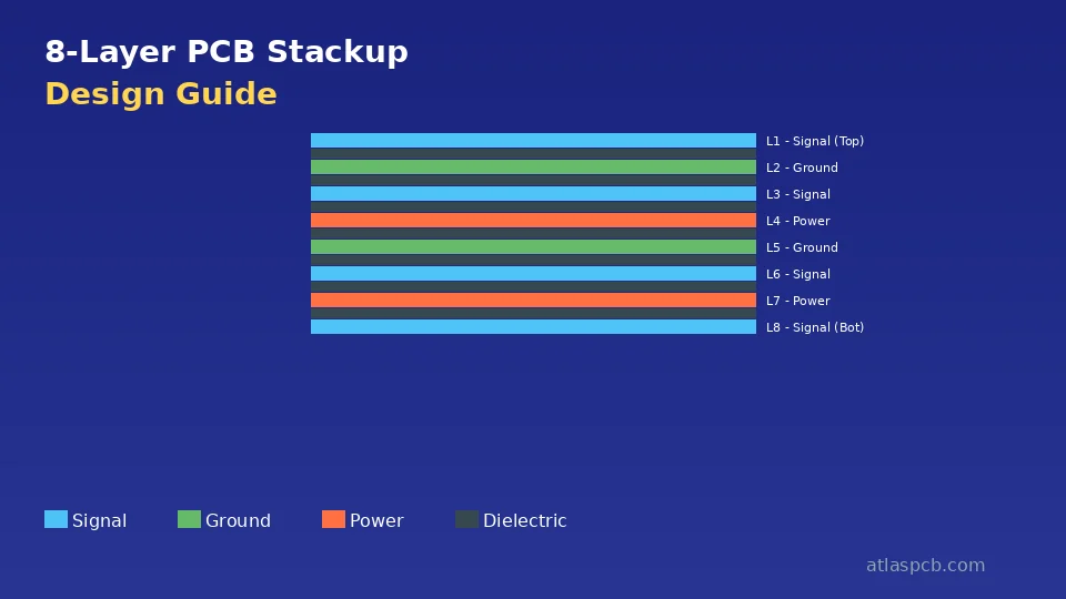
For an 8-layer DDR5 stackup, the recommended layer assignment places signals on layers 1, 3, 6, and 8, with ground planes on layers 2, 4, 5, and 7. The signal-to-reference dielectric thickness should target 3.5 to 4.5 mils depending on the material system and target impedance. For a 40 ohm single-ended target in Megtron 4 (Dk approximately 3.8 at 10 GHz), this typically requires a trace width of 3.5 to 4.0 mils on inner stripline layers with a dielectric spacing of 3.8 to 4.2 mils to the adjacent ground plane. Outer microstrip layers achieve 40 ohms with approximately 4.5 to 5.0 mil trace width over a 3.5 mil dielectric.
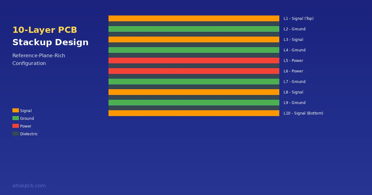
A 12-layer stackup provides more routing flexibility for complex DDR5 implementations. The typical configuration uses signal layers on 1, 3, 5, 8, 10, and 12, with ground planes on layers 2, 4, 6, 7, 9, and 11. The ground-ground plane pair at layers 6 and 7 provides excellent high-frequency decoupling capacitance and serves as the ideal power distribution reference for the memory interface. This configuration ensures every signal layer has an immediately adjacent ground reference while maintaining stackup symmetry to prevent warpage during lamination.
When specifying your stackup to the manufacturer, provide target dielectric thicknesses rather than fixed values. A specification of 4.0 mils plus or minus 0.3 mils gives the fabricator enough process latitude to achieve consistent results while maintaining your impedance targets. Overly tight dielectric specifications (plus or minus 0.1 mil) often force the manufacturer into multiple lamination iterations, driving up cost without meaningful signal integrity benefit. The impedance outcome matters more than the individual dielectric dimension.
AtlasPCB provides free stackup engineering review for DDR5 designs. Our SI team validates impedance targets, material selection, and dielectric dimensions before production begins. Submit your design for review
Material Selection: Matching Loss Budget to Data Rate
Standard FR-4 laminates with dissipation factors above 0.015 at 10 GHz are fundamentally incompatible with DDR5 signal integrity requirements. At 6400 MT/s, the fundamental clock frequency reaches 3.2 GHz, with signal energy extending to the third and fifth harmonics at 9.6 and 16 GHz respectively. At these frequencies, the dielectric loss of standard FR-4 produces insertion loss exceeding 1.0 dB per inch on inner stripline layers, which rapidly closes the timing eye and exhausts receiver equalization budget.
The practical material tiers for DDR5 break down as follows. For short DDR5 channels under 3 inches total routing length at data rates up to DDR5-4800, mid-loss materials with Df in the 0.005 to 0.009 range at 10 GHz provide adequate performance. This tier includes Panasonic Megtron 4 (Df approximately 0.005), Isola FR408HR (Df approximately 0.009), Shengyi S1000-2M (Df approximately 0.008), and TUC TU-872 SLK (Df approximately 0.006). These materials typically cost 1.5 to 2.5 times standard FR-4 pricing and are available with reasonable lead times from most laminate distributors.
For longer DDR5 channels exceeding 4 inches, data rates at DDR5-5600 and above, or designs requiring maximum timing margin, low-loss materials with Df below 0.005 at 10 GHz become necessary. This tier includes Panasonic Megtron 6 (Df approximately 0.002), Isola I-Speed (Df approximately 0.005), Isola I-Tera MT40 (Df approximately 0.003), and EM-890K (Df approximately 0.003). These materials carry a 3 to 4 times cost premium over standard FR-4 and may require longer procurement lead times, particularly for Megtron 6 which has faced consistent allocation constraints driven by AI server demand throughout 2026.
Copper foil selection significantly impacts DDR5 signal loss at frequencies above 5 GHz. Standard electrodeposited copper with an Rz roughness of 5 to 8 micrometers can add 0.3 to 0.5 dB per inch of loss at 10 GHz due to skin effect interaction with surface roughness. Specifying HVLP (hyper-very-low-profile) or RTF (reverse-treated foil) copper with Rz below 2 micrometers reduces this penalty to under 0.1 dB per inch. The cost premium for smooth copper is modest (5 to 15 percent of material cost) but the signal integrity benefit at DDR5 frequencies is substantial.
Glass weave selection matters for DDR5 because the periodic structure of woven fiberglass creates localized dielectric constant variation. A trace routed over a glass bundle sees a different Dk than a trace routed over a resin-rich channel between bundles, creating impedance variation and propagation delay skew between adjacent traces. For DDR5 byte lanes where 5-mil length matching equates to 2.5 picoseconds timing budget, fiber weave-induced skew can consume a meaningful fraction of that margin. Spread glass styles like 1078 and 1086 minimize this effect by distributing glass filaments more uniformly and reducing the delta between glass-rich and resin-rich regions. Specifying spread glass on signal layers adds approximately 5 to 10 percent to material cost but eliminates a significant source of intra-byte-lane timing variation. For more detail on prepreg selection, see our guide on glass weave and resin content for impedance control.
Routing and Length Matching: The Manufacturing Perspective
The fly-by topology mandated for DDR5 address and command signals means these traces visit each DRAM device sequentially in a daisy chain. From a fabrication standpoint, this topology creates long continuous traces that span the full memory channel length, making them particularly sensitive to impedance uniformity along their path. Any fabrication-induced impedance variation from etch inconsistency, dielectric thickness drift, or reference plane copper density changes creates distributed reflections that accumulate along the fly-by chain.
Byte-lane length matching within 5 mils requires serpentine tuning structures with specific geometric constraints. The serpentine pitch (center-to-center spacing between adjacent meander segments) must be at least 5 times the trace width to prevent self-coupling between segments. For a 4-mil-wide DDR5 data trace, this means serpentine pitch of 20 mils minimum. Tighter serpentine creates capacitive coupling between segments that alters the effective electrical length, potentially worsening the matching it was intended to achieve.
Differential pair routing for DQS strobes and CK clock signals demands consistent edge-to-edge spacing along the entire route. Manufacturing variation in differential pair spacing directly impacts differential impedance. A 1-mil spacing variation on a pair with 5-mil nominal gap produces approximately a 3 to 4 ohm impedance shift. This translates directly into the plus or minus 5 percent tolerance budget for 100 ohm differential pairs. The fabrication process must maintain pair spacing consistency below plus or minus 0.5 mils to leave adequate margin for other tolerance contributors.
One of the most common DFM issues we encounter in DDR5 designs is inconsistent reference plane copper density beneath signal routing. When ground planes contain large clearance voids around through-hole vias, mounting holes, or component pads, the effective reference plane distance from the signal trace changes locally, creating impedance discontinuities. Our engineering review specifically checks for reference plane continuity beneath all DDR5 signal routing and flags areas where the effective ground plane copper fill drops below 70 percent within a 50-mil radius of any signal trace.
Via Strategy and Stub Management
Via stubs in DDR5 boards create quarter-wave resonances that produce insertion loss notches at specific frequencies. A 40-mil via stub in standard FR-4 (Dk approximately 4.2) creates a resonance at approximately 18 GHz, which falls within the bandwidth of DDR5-6400 signals. A longer 60-mil stub drops the resonance to approximately 12 GHz, directly impacting signal energy at the third harmonic of DDR5-4800. The practical maximum via stub length for DDR5 designs is 10 mils, which places the resonance above 70 GHz where it has negligible impact on signal integrity.
Back-drilling (controlled-depth drilling) removes via stubs by boring out the unused portion of a plated through-hole from the opposite side. For a 12-layer DDR5 board where a signal transitions from layer 3 to layer 10, a through-hole via extends from layer 1 to layer 12. The stub from layer 1 to layer 3 and from layer 10 to layer 12 must be removed. Back-drilling from both sides achieves this, but the process has a depth tolerance of approximately plus or minus 4 to 6 mils. Your fabrication drawing should specify a maximum remaining stub length of 8 to 10 mils to accommodate this drilling tolerance while keeping the effective stub short enough for DDR5 signal integrity.
Blind and buried vias eliminate stubs entirely by terminating the via at the target layer. A blind via from layer 1 to layer 3 has zero stub. The cost premium for blind vias compared to back-drilled through-holes is typically 20 to 35 percent of the total board cost, which is higher than back-drilling (10 to 20 percent premium) but provides deterministic stub elimination without drilling tolerance uncertainty. For designs operating at DDR5-5600 and above where stub control is most critical, blind vias offer the most reliable manufacturing solution.
For BGA breakout beneath DDR5 DRAM devices and connectors, laser-drilled microvias (0.1 to 0.15mm diameter) provide the minimum impedance disruption during layer transitions. The small via diameter and thin dielectric span of microvias create much lower capacitive loading than conventional through-hole vias, which is particularly important for the dense signal fields under fine-pitch BGA packages. Our standard DDR5 fabrication process uses microvias for all signal transitions within the BGA field and reserves through-hole vias (with back-drilling) for transitions outside the BGA footprint where space permits larger drill diameters. For more on via stub impact and back-drilling specifications, see our detailed guide on PCB back-drilling and via stub removal for signal integrity.
Not sure whether your DDR5 design needs back-drilling, blind vias, or microvias? Our engineering team evaluates your via strategy against signal integrity requirements and recommends the most cost-effective approach. Get a free DFM review
Manufacturing Tolerances That Matter for DDR5
Achieving plus or minus 5 percent impedance tolerance on 40 ohm single-ended traces means the manufactured impedance must fall between 38 and 42 ohms. In practical terms, this requires trace width control to plus or minus 0.3 mils, dielectric thickness control to plus or minus 0.3 mils, and Dk variation within plus or minus 3 percent across the panel. Standard fabrication processes typically achieve trace width tolerance of plus or minus 0.5 to 0.7 mils, which translates to approximately plus or minus 7 to 10 percent impedance variation on 40 ohm targets. Meeting DDR5’s tighter requirement demands premium process controls.
The etch factor becomes particularly critical for the fine traces used in DDR5 routing. At 3.5 to 4.0 mil trace widths, the trapezoidal profile produced by chemical etching creates a measurable difference between top width (at the etch resist) and bottom width (at the copper-dielectric interface). Our manufacturing process accounts for this by applying etch compensation factors of 0.5 to 0.8 mils depending on copper weight to the photolithography artwork, ensuring the finished trace width at the measurement point matches the impedance simulation target. For detailed information on how etch compensation affects trace width and impedance, refer to our article on PCB etch factor and trace width compensation.
Layer-to-layer registration accuracy matters for DDR5 designs because via-to-pad alignment in fine-pitch BGA fields determines whether the via capture pad fully encloses the drilled hole. Misregistration can expose the drill hole outside the pad boundary, creating a void in the copper barrel that degrades via impedance and reliability. For DDR5 BGA packages with 0.5mm pitch requiring 8-mil capture pads and 4-mil drill holes, the registration tolerance budget allows only plus or minus 2 mils before the pad no longer fully encloses the hole. Standard fabrication achieves plus or minus 2 to 3 mils layer registration, meaning DDR5 designs at fine pitch require the manufacturer to hold the tight end of their process capability.
How DDR5 Specifications Affect PCB Cost
DDR5-grade PCB fabrication carries a meaningful cost premium that designers should factor into their BOM estimates early in the design cycle. Based on our production data across hundreds of DDR5 board designs, the typical cost breakdown compared to an equivalent standard-tolerance board follows a predictable pattern.
Material cost contributes the largest premium. Low-loss laminates run 2 to 4 times the cost of standard FR-4, and this material cost applies to every layer of the stackup even if only two signal layers carry DDR5 traces. A typical 8-layer DDR5 board using Megtron 4 throughout sees material cost approximately 2 times higher than the same stackup in standard Shengyi S1000. Using Megtron 6 pushes this to 3 to 3.5 times.
Process cost additions come from tighter etch control requiring slower etch lines with tighter chemistry monitoring, 100 percent AOI on inner layers versus sampling, controlled-depth back-drilling adding a separate drilling operation with specialized equipment, and additional impedance coupon testing with TDR verification on every production panel rather than lot sampling. Collectively, these process additions add 15 to 30 percent to fabrication cost beyond the material premium.
Yield impact further increases effective cost. Tighter impedance specifications mean more panels fail final test and must be scrapped. At plus or minus 10 percent tolerance on standard boards, our first-pass impedance yield exceeds 95 percent. At plus or minus 5 percent for DDR5, first-pass yield typically drops to 85 to 90 percent, and the cost of scrapped panels is distributed across shipped boards.
The total cost premium for a DDR5-grade 8-layer board compared to an equivalent standard board typically falls in the 30 to 60 percent range. A board that would cost 100 dollars in standard fabrication becomes 130 to 160 dollars with DDR5 specifications. Understanding this cost impact upfront allows designers to make informed decisions about where to apply DDR5-grade specifications and where standard tolerances suffice. Signal layers carrying DDR5 routing genuinely need the tight tolerances. Power planes and low-speed I/O layers in the same board may not.
What to Include in Your DDR5 Fabrication Drawing
Your fabrication drawing is the contractual specification that determines what your manufacturer builds. For DDR5 boards, incomplete or ambiguous specifications are the primary source of manufacturing issues we encounter. A complete DDR5 fabrication package should include the following specifications.
Impedance specifications must state explicit target values with tolerances for each controlled impedance structure. Simply noting controlled impedance without values forces the manufacturer to guess or contact you for clarification, adding days to your timeline. Specify each impedance class separately: 40 ohm plus or minus 5 percent single-ended for data and address signals, 100 ohm plus or minus 5 percent differential for clock and strobe pairs, and identify which layers carry each impedance class.
Material specification should call out approved laminate grades by manufacturer and product name, not generic terms. A note stating FR-4 allows the fabricator to use any standard laminate, which may not meet your Dk and Df requirements. Instead, specify acceptable materials explicitly: Panasonic Megtron 4, Isola FR408HR, or equivalent with Dk 3.6 to 3.9 and Df below 0.009 at 10 GHz. This gives the manufacturer procurement flexibility while ensuring performance.
Via stub specification should state the maximum acceptable stub length after back-drilling, typically 8 to 10 mils for DDR5. Include a drilling detail showing which vias require back-drilling, from which side, and to what depth. Note the specific signal layers that set the back-drill depth target.
The stackup drawing should show all layers with target dielectric thicknesses, copper weights per layer, prepreg and core specifications, and total board thickness. Mark which layers are controlled-impedance and reference the impedance table. Include symmetry requirements if warpage is a concern.
Impedance coupon requirements should specify testing per IPC-TM-650 method 2.5.5.7 with TDR method, state the required coupon structures matching each impedance class in the design, and note whether 100 percent panel testing or lot sampling is acceptable.
AtlasPCB specializes in controlled impedance boards with tight-tolerance manufacturing. Our engineering team reviews every DDR5 design before production to catch DFM issues early and optimize your specifications for cost and yield. Get a quote for your DDR5 board
Common DDR5 DFM Issues from Our Production Floor
After processing several hundred DDR5 designs through our engineering review, certain failure patterns emerge repeatedly. Understanding these common issues helps designers avoid the most frequent causes of DDR5 board failures and manufacturing delays.
The most frequent issue is material specification mismatch, where designers submit DDR5 boards with no material callout or a generic FR-4 specification. Standard FR-4 with Df of 0.018 to 0.022 produces insertion loss exceeding 1.2 dB per inch on inner-layer stripline at DDR5 frequencies. This level of loss typically closes the timing eye below usable margins even with receiver equalization active. Our engineering review flags this immediately and recommends appropriate material grades based on the specific channel length and data rate in the design.
Missing impedance tolerance specification is the second most common issue. When a fabrication drawing notes controlled impedance at 40 ohms without stating a tolerance, the manufacturer applies their standard tolerance, which is typically plus or minus 10 percent. For DDR5, this allows the manufactured impedance to range from 36 to 44 ohms, which may be inadequate for signal integrity at higher data rates. Explicitly specifying plus or minus 5 percent or plus or minus 7 percent ensures the manufacturer applies the appropriate process controls.
Absence of back-drill callouts on through-hole vias carrying DDR5 signals creates via stubs that degrade signal integrity at frequencies above 5 GHz. Many designers transitioning from DDR4, where stubs were less problematic due to lower bandwidth requirements, forget to add back-drill specifications to their DDR5 fabrication notes. Our review identifies all through-hole vias on DDR5 signal nets and recommends back-drilling where stubs exceed 10 mils.
Reference plane discontinuities beneath DDR5 routing remain surprisingly common. Split power planes, large thermal relief patterns on ground vias, and clearance voids from through-hole component pins can create gaps in the reference plane directly under signal traces. These gaps alter the local impedance by 5 to 15 ohms depending on gap size and proximity, creating reflections that degrade signal quality. Our CAM review uses automated DRC to verify continuous reference plane coverage within 50 mils of all controlled-impedance traces.
Insufficient spacing between byte lanes allows far-end crosstalk to couple between adjacent data groups, introducing timing noise that corrupts the sampling relationship between DQ and DQS signals. DDR5 designs should maintain at least 20 mils (approximately 5 times trace width) between adjacent byte lanes. Designs that compress byte-lane spacing to save routing area often fail signal integrity verification during production testing.
For related discussion of differential impedance control methods applicable to DDR5 clock and strobe routing, see our detailed technical article on differential impedance for PCIe Gen5 and DDR5.
Reviewed by AtlasPCB Engineering Team
About AtlasPCB — We specialize in complex PCB manufacturing for HDI, RF, and high-reliability applications. Explore our impedance-controlled PCB manufacturing, Megtron 6 & 7 low-loss PCB manufacturing, or get an free engineering DFM review . Every order includes free engineering review. Get your quote.
Reviewed by AtlasPCB Engineering Team — IPC-certified manufacturing specialists with 15+ years of production experience in HDI, RF, and high-reliability PCB fabrication. Content based on factory floor data and real customer design reviews.
Frequently Asked Questions
What impedance do DDR5 signals require?
What PCB material should I use for DDR5?
How many PCB layers do I need for DDR5?
How much more does a DDR5 PCB cost compared to standard boards?
What should I specify in my fab drawing for DDR5 boards?
- DDR5
- PCB design
- signal integrity
- impedance control
- PCB stackup
- high-speed routing
- PCB manufacturing
- DFM