· AtlasPCB Engineering Team · Engineering · 16 min read
Conformal Coating vs Potting Compound: PCB Protection Methods Compared
In-depth comparison of conformal coating and potting for PCB protection. Covers material selection, DFM design rules, thermal impact, IPC qualification standards, production costs, and when to use a hybrid approach for maximum reliability.
Quick Answer
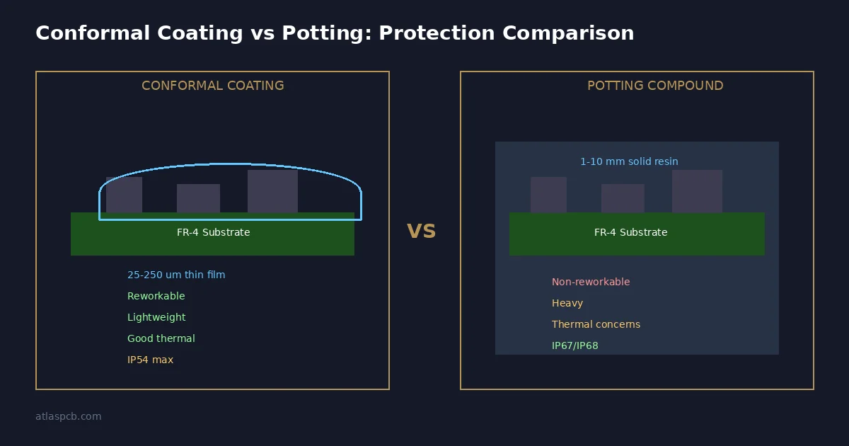
Conformal coating applies a thin (25-250 µm) polymer film that protects PCBs against moisture and contamination while preserving reworkability and adding negligible weight. Potting fully encapsulates the assembly in 1-10 mm of resin, providing superior mechanical, vibration, and IP68-level protection at the cost of increased weight, no reworkability, and higher per-unit expense. The optimal choice depends on environmental severity, thermal constraints, production volume, and serviceability requirements.
How Conformal Coating and Potting Protect PCBs Differently
Every electronics engineer faces the same question when designing for harsh environments: should the PCB assembly receive a conformal coating, full potting, or some combination of both? The answer affects not just environmental protection but also thermal management, serviceability, production cost, and even the PCB layout itself.
Conformal coating creates a thin polymeric barrier — typically 25 to 250 micrometers thick — that conforms to the topography of components, traces, and solder joints. Think of it as a second skin that breathes with the board while blocking moisture ingress, ionic contamination, and fungal growth. The board remains visible, accessible for rework, and thermally connected to the surrounding air.
Potting takes the opposite philosophy. The entire PCB assembly is encapsulated in 1 to 10 millimeters of cured resin, creating a monolithic block that mechanically locks every component in place. Nothing gets in or out. The board becomes impervious to vibration, mechanical shock, water immersion, and even reverse engineering attempts. However, it also becomes a sealed thermal mass that cannot be inspected or reworked.
From a manufacturing perspective at Atlas PCB, the protection method decision must happen early in the design phase — not after layout completion. Both approaches impose specific design constraints that, if ignored, result in production delays, yield issues, or compromised protection coverage.
Material Options and Performance Properties
Conformal Coating Materials
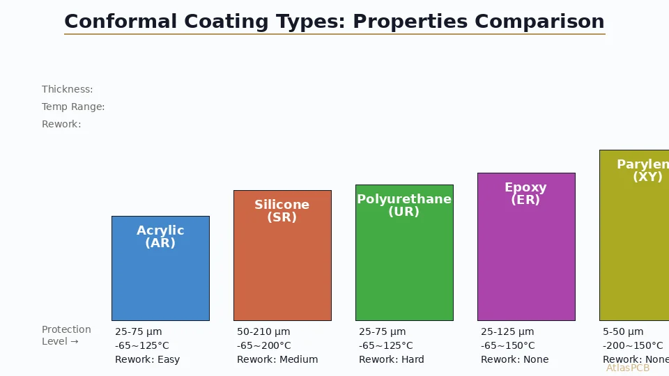
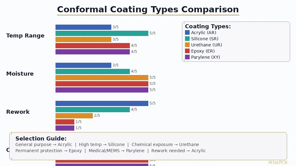
The five primary conformal coating chemistries each serve distinct application profiles. Acrylic coatings (Type AR per IPC-CC-830) offer the simplest processing — they cure at room temperature and dissolve in common solvents for easy rework. Their moisture resistance is adequate for consumer and light industrial applications operating between minus 40 and plus 125 degrees Celsius.
Silicone coatings (Type SR) excel in extreme temperature ranges, maintaining flexibility from minus 65 to plus 200 degrees Celsius. This makes them the default choice for automotive underhood electronics and aerospace applications where thermal cycling would crack rigid coating materials. Their dielectric strength exceeds 20 kV per millimeter, providing excellent high-voltage isolation.
Polyurethane coatings (Type UR) deliver the strongest chemical resistance of any easily applied coating, withstanding prolonged exposure to fuels, solvents, and aggressive cleaning agents. They cure harder than silicone but softer than epoxy, providing a useful middle ground for industrial control equipment. However, their maximum operating temperature of 130 degrees Celsius limits aerospace applicability.
Parylene coatings (Type XY) are unique — deposited as a vapor in a vacuum chamber, they produce an ultra-thin, pinhole-free barrier with unmatched thickness uniformity. At just 5 to 50 micrometers, parylene adds virtually zero stress to delicate wire bonds and MEMS structures. The trade-off is cost: vacuum deposition equipment and batch processing make parylene three to ten times more expensive per board than spray-applied alternatives.
Epoxy coatings (Type ER) provide the hardest, most abrasion-resistant surface but sacrifice flexibility entirely. Once cured, they cannot be removed without mechanical abrasion, making rework essentially impossible. Their use is limited to applications where the coating must resist physical abrasion and the board is considered non-repairable.
Potting Compound Materials
Potting compounds use similar base chemistries — epoxy, silicone, and polyurethane — but in much thicker cross-sections that fundamentally change their performance characteristics.
Epoxy potting compounds cure to shore D hardness of 70 to 90, creating a rigid mass with excellent compressive strength (80 to 150 MPa) and chemical resistance. They provide strong adhesion to FR-4 substrates and component bodies, mechanically reinforcing solder joints against vibration fatigue. Standard epoxy potting has thermal conductivity of 0.2 to 0.5 W/mK, while filled formulations reach 1.0 to 1.5 W/mK for improved heat transfer.
Silicone potting compounds remain flexible after cure (shore A hardness 20 to 60), making them ideal for applications subject to repeated thermal cycling or mechanical flexing. Their thermal conductivity ranges from 0.2 W/mK for standard grades to 2.0 W/mK for thermally loaded formulations. Silicone’s coefficient of thermal expansion closely matches common PCB materials, reducing interfacial stress during temperature excursions.
Polyurethane potting offers a middle path — semi-rigid cure (shore A 60 to shore D 50), good adhesion, and excellent moisture resistance. It costs less than silicone and processes more easily than high-performance epoxy systems, making it popular for mid-volume industrial products operating in moderately harsh conditions.
Application Process and Production Impact
The application method directly impacts production throughput, which matters when planning PCBA lead times and manufacturing costs.
Conformal coating application typically adds 2 to 4 hours to the production cycle when including cure time. Selective robotic coating — where a programmable dispenser traces predetermined paths while avoiding connectors and test points — achieves cycle times of 30 to 90 seconds per board with minimal masking. Spray coating handles high volumes quickly but requires extensive masking of keep-out areas. Dip coating provides the most uniform coverage but offers the least selectivity.
Potting fundamentally changes the production sequence. The PCB assembly must be placed into a pre-manufactured housing or mold, the mixed compound is dispensed (often under vacuum to prevent trapped air bubbles), and then the assembly enters a cure cycle lasting 4 to 72 hours depending on compound chemistry and section thickness. This extended cycle time means potted assemblies typically require dedicated curing ovens or racks, adding significant floor space and work-in-progress inventory to the manufacturing operation.
At production volumes above 5000 units per month, automated selective conformal coating becomes the clear winner for throughput efficiency. Potting remains practical for volumes up to a few thousand units monthly, beyond which the cure time bottleneck requires either parallel processing lines or faster-curing (and more expensive) compound formulations.
DFM Design Rules for PCB Protection
This is where our fabrication experience adds the most value. We regularly review customer designs that specify conformal coating or potting but haven’t accounted for the manufacturing requirements of each method.
Design Rules for Conformal Coating
Proper conformal coating requires the PCB designer to define keep-out areas — zones that must remain uncoated for the assembly to function correctly. These include all mating surfaces of board-to-board connectors, test points and programming headers that require probe access, press-fit connector areas where coating would compromise the mechanical interface, thermal interface surfaces where the board contacts a heatsink or chassis, and any switch or button mechanisms.
The PCB silkscreen layer should clearly mark the coating boundary line, and fab drawings must specify coating keep-out dimensions with at least 1.5 millimeter clearance from connector pin rows. We recommend designing a dedicated manufacturing layer in your CAD tool that defines the coating boundary — this layer translates directly to the selective coating machine’s programming file.
Component height variation affects coating thickness uniformity. Tall components (greater than 10 millimeters) create shadowing effects during spray application, potentially leaving thin coverage on adjacent low-profile components. When the design includes both tall electrolytics and low-profile passives in close proximity, specify dip coating or dual-pass spray to ensure minimum thickness compliance.
Design Rules for Potting
Potting imposes different constraints. The PCB must fit within a housing or mold with specific clearances: minimum 2 millimeters between the highest component and the top of the potting level to ensure full encapsulation, minimum 1 millimeter clearance between board edges and housing walls for compound flow, and all cable entry points must accommodate strain relief within the potted volume.
Critical DFM consideration: components with trapped air cavities — such as unsealed electrolytic capacitors, some relay packages, and certain connector housings — can trap bubbles during potting that expand during thermal cycling, eventually cracking the compound or damaging the component. These components must either be pre-sealed, replaced with solid-construction alternatives, or positioned above the potting level.
The housing or dam material must be chemically compatible with the potting compound and able to withstand the exothermic cure temperature. Aluminum housings work universally. ABS and polycarbonate plastics are compatible with most silicone and polyurethane compounds but may warp from epoxy cure temperatures exceeding 80 degrees Celsius.
DFM ENGINEERING REVIEW
Get Your Design Reviewed for Coating Compatibility
Our engineering team identifies keep-out conflicts, component clearance issues, and thermal risks before production begins.
Upload Design Files ›
Thermal Management Considerations
The thermal implications of PCB protection are frequently underestimated. A thin conformal coating (25-75 micrometers) has negligible thermal resistance — less than 0.1 degrees Celsius per watt for a typical component footprint. The board continues to dissipate heat through convection and radiation almost as effectively as an uncoated assembly.
Potting creates a fundamentally different thermal environment. Standard epoxy potting (thermal conductivity 0.3 W/mK) surrounding a component that dissipates 2 watts through a 1 square centimeter footprint adds approximately 6.7 degrees Celsius of thermal resistance per millimeter of potting thickness above the component. For a typical 3 millimeter potting depth above a power IC, this translates to a 20 degree Celsius junction temperature increase — potentially pushing components beyond their rated operating range.
The solution is material selection and thermal path design. Thermally conductive potting compounds (1.0 to 2.0 W/mK) cut this temperature rise by three to six times. Additionally, designing the PCB with thermal vias beneath high-power components that connect to a copper ground plane pressing against the metal housing creates a direct thermal path that bypasses the potting compound entirely. This design technique — thermal vias to chassis ground through the board bottom — is standard practice for potted automotive and industrial power electronics.
When we review customer designs for potted assemblies, thermal simulation is the first step. We model the expected junction temperatures with the proposed potting compound and verify that all components remain within their absolute maximum ratings with appropriate derating applied.
Reliability Standards and Qualification Testing
Understanding which standards apply helps specify protection requirements correctly on your assembly drawing.
Conformal coatings are qualified per IPC-CC-830C, which replaced the military specification MIL-I-46058C. This standard defines five material groups (AR, SR, UR, ER, XY) and specifies testing for insulation resistance after 10 days at 90 percent relative humidity (minimum 100 megohms), thermal shock resistance across 500 cycles from minus 65 to plus 125 degrees Celsius, dielectric withstanding voltage (minimum 1500 V DC at sea level), flexibility after aging (no cracking on 6.35 millimeter mandrel bend), and fungus resistance per ASTM G21.
Potting compounds do not have a single unified qualification standard equivalent to IPC-CC-830. Instead, they are characterized by a combination of standards: UL 94 flammability classification (typically V-0 required for potted electronics), ASTM D2240 for shore hardness characterization, ASTM D149 for dielectric breakdown voltage, and UL 746E for polymeric materials used in printed wiring board assemblies.
For potted assemblies destined for outdoor or wash-down environments, the complete assembly is typically tested to IEC 60529 for Ingress Protection rating. Properly designed potted enclosures routinely achieve IP67 (temporary immersion) or IP68 (continuous submersion) ratings that are virtually impossible to achieve with conformal coating alone.
Military applications may reference MIL-STD-810H for environmental testing of the complete potted assembly, including Method 501.7 (high temperature), Method 502.7 (low temperature), Method 507.6 (humidity), and Method 514.8 (vibration).
Cost Analysis by Production Volume
Cost is often the deciding factor between conformal coating and potting. Here is what we see in actual production scenarios at different volume tiers.
For conformal coating, the cost breakdown includes material cost of $0.10 to $0.50 per board depending on board size and coating type, masking labor or fixture amortization of $0.20 to $1.00 per board, application labor or machine time of $0.15 to $0.50 per board, and cure cycle overhead of $0.05 to $0.20 per board. Total per-board cost ranges from $0.50 for high-volume automated selective coating to $3.00 for low-volume manually masked spray coating. Initial tooling investment for masking fixtures runs $200 to $500.
For potting, material cost runs $0.80 to $5.00 per board depending on compound volume and type. Custom mold or housing tooling costs $500 to $3000 amortized over production run. Dispensing and vacuum degassing labor adds $0.50 to $2.00 per board. Cure cycle time (occupying oven space) adds $0.30 to $1.00 per board. Total per-board cost ranges from $2.00 for simple dam-and-fill with standard epoxy to $15.00 or more for vacuum-potted silicone in custom CNC-machined aluminum housings.
The volume crossover point where automated selective conformal coating becomes dramatically cheaper than potting occurs around 1000 to 2000 units. Below 100 units, the cost difference is less significant because both methods involve manual processing, but the potting mold investment makes it relatively more expensive for very small runs.
PROTECTED ASSEMBLY PRICING
Get Itemized Quotes for Coating, Potting, or Hybrid Protection
Upload your design files and specify protection requirements. We provide cost breakdowns for all three approaches within 24 hours.
Get Assembly Quote ›The Hybrid Approach: Combining Both Methods
In our production experience, approximately 15 percent of protected assemblies use a hybrid approach — conformal coating across the entire board plus local potting of specific high-stress areas. This combination captures the advantages of both methods while minimizing their individual limitations.
A typical hybrid application starts with selective conformal coating of the entire PCB assembly, protecting all components and solder joints against moisture and contamination while maintaining thermal performance and visual inspectability. Then, specific areas receive local potting: cable entry strain reliefs where mechanical stress concentrates, exposed connector interfaces in outdoor-rated products, high-power sections where thermally conductive potting aids heat transfer to the enclosure, and vibration-sensitive components like crystal oscillators or MEMS sensors.
Automotive engine control units frequently use this approach. The main processor and memory section receives silicone conformal coating for temperature flexibility and reworkability during production testing, while the wiring harness connector area gets polyurethane potting for vibration resistance and IP67 sealing at the cable entry point.
Outdoor IoT sensor nodes are another common application. The radio and processor section is conformally coated (enabling firmware updates through debug connectors), while the antenna feedthrough and power cable entry are locally potted for water ingress protection.
The key design requirement for hybrid protection is clear documentation. The assembly drawing must specify exactly which areas receive coating only, which receive potting, and what the interface zone between the two methods looks like. We recommend a minimum 5 millimeter uncoated transition zone between coated and potted regions to prevent adhesion failure at the interface.
Decision Framework: Choosing the Right Protection Method
Rather than presenting a generic flowchart, here is how we guide customers through this decision based on their actual application requirements.
Choose conformal coating when the operating environment involves humidity and condensation but not direct water exposure, when the product requires field serviceability (component replacement, firmware programming, or production test access), when weight and size constraints limit additional material mass (portable devices, drones, wearables), when production volumes exceed 5000 units and cost optimization matters, or when thermal dissipation must remain unimpeded (high-power processors, LED arrays, power converters without heatsink contact).
Choose potting when the assembly faces continuous vibration or mechanical shock (industrial motors, vehicle-mounted equipment, handheld power tools), when IP67 or IP68 water immersion protection is required without an additional sealed enclosure, when intellectual property protection against reverse engineering is a concern, when high-voltage isolation requires bulk dielectric material (power supplies above 1000V, ignition systems), or when the product is designed as a sealed, non-serviceable module with defined replacement intervals.
Choose the hybrid approach when different areas of the same assembly face different environmental stresses, when you need a serviceable main board but sealed cable/connector interfaces, when thermal management requires selective protection (coat most areas, use thermally conductive potting only where needed), or when regulatory compliance requires IP-rated sealing at specific ingress points while maintaining internal repairability for other regions.
ATLASPCB
Not Sure Which Protection Method Fits Your Application?
Our engineering team evaluates your environment, thermal constraints, and production targets to recommend the most effective protection strategy. Over 2000 protected assemblies delivered across automotive, industrial, and IoT applications.
Discuss Your Requirements ›
Environmental Compliance and Material Trends
The regulatory landscape is shifting protection material choices in 2026. The European Union’s proposed PFAS restriction under REACH affects certain fluoropolymer-based conformal coatings that have historically offered superior chemical resistance and low surface energy. While the restriction timeline extends to 2027 for electronics applications, forward-thinking designers are already specifying PFAS-free alternatives — particularly parylene C (which is not a PFAS compound) and modified silicone formulations.
For potting compounds, the primary compliance consideration is RoHS and halogen-free requirements. Most modern potting compounds already meet these requirements, but legacy epoxy formulations containing brominated flame retardants are still available and must be explicitly excluded from procurement specifications for EU-bound products.
The industry trend is toward bio-based and recyclable potting compounds. While current options have limited performance compared to petroleum-derived resins, development of castor-oil-based polyurethane and plant-derived epoxy systems is progressing rapidly. For applications where potted modules will eventually require disposal, specifying thermally reversible potting compounds (which soften above 150 degrees Celsius for component recovery) supports circular economy objectives without compromising operational reliability.
Conclusion
The choice between conformal coating and potting is ultimately a systems engineering decision that balances protection requirements against thermal constraints, serviceability needs, production economics, and regulatory compliance. Neither method is universally superior — each serves distinct applications optimally.
What separates successful protected assemblies from field failures is the integration of protection planning into the earliest stages of PCB design. Layout decisions made during schematic and placement — including component spacing and DFA rules — directly determine whether the chosen protection method can be applied effectively, affordably, and with consistent quality at production volume.
Reviewed by AtlasPCB Engineering Team — 15+ years in advanced PCB fabrication for RF, HDI, and rigid-flex applications.
Related Reading:
About AtlasPCB — We specialize in complex PCB manufacturing for HDI, RF, and high-reliability applications. Explore our PCB assembly services, free engineering DFM review, or get an full PCB manufacturing capabilities . Every order includes free engineering review. Get your quote.
Reviewed by AtlasPCB Engineering Team — IPC-certified manufacturing specialists with 15+ years of production experience in HDI, RF, and high-reliability PCB fabrication. Content based on factory floor data and real customer design reviews.
Frequently Asked Questions
What is the cost difference between conformal coating and potting?
Can you use both conformal coating and potting on the same PCB?
Does potting compound affect PCB thermal performance?
What IPC standards apply to conformal coating and potting?
- conformal coating
- potting compound
- PCB protection
- IPC-CC-830
- DFM
- harsh environment electronics
- PCB assembly